Quantum computers are poised to revolutionize fields such as cryptography, biology, and medicine by vastly outperforming classical computers in problem solving. The key to their advantage lies in qubits, fundamental units of quantum information, which can exist in multiple states simultaneously, enabling the execution of completely different algorithms.
However, unlocking their full potential necessitates the coordinated operation of hundreds or even thousands of qubits over extended periods. This has proven challenging because qubits’ quantum states are easily disrupted by their environment.
A research team has proposed a novel solution to this problem: creating scalable quantum computers where qubits are defects within a silicon crystal lattice.
“To make a scalable quantum architecture or network, we need qubits that can reliably form on-demand, at desired locations, so that we know where the qubit is located in a material. And that’s why our approach is critical,” Kaushalya Jhuria, a postdoctoral scholar at Berkeley Lab’s Accelerator Technologies and Applied Physics (ATAP) Division and lead author of the study, said in a press release. “Because once we know where a specific qubit is sitting, we can determine how to connect this qubit with other components in the system and make a quantum network.”
Quantum computing with lattice defects
Defects in a crystal lattice occur when atoms are displaced from their regular positions within a material, which leads to a change in the properties of their interaction with neighboring atoms and the nuclei of the defect atoms with their electrons.
These changes could make some atomic quantum states easily addressable and controlled, meaning that defects can be used to store and manipulate quantum information, making them potential candidates for qubits.
In recent years, developing quantum computers based on silicon defects has gained traction as the properties of their quantum states result in their well-defined emission frequency and good brightness, and their ability to emit single photons, which enables reliable communication.
However, building a functional quantum computer using this method has been challenging. Traditional qubit formation involves high-temperature treatment, or annealing, of thin slices of silicon, known as wafers, in a special furnace. Annealing the wafer randomly forms qubits, but this randomness makes it difficult to ensure controlled and reliable interactions between the qubits.
Laser annealing comes to the rescue
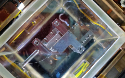
In their study published in Nature Communications, the team proposed an innovative method to refine this technology. They used a femtosecond laser pulse to locally anneal a carbon-doped silicon wafer in the presence of hydrogen, which creates defects at precise locations and integrates hydrogen atoms into them, enhancing their suitability as qubits.
The quality of the defect improved because the interaction of an additional hydrogen atom with the silicon and carbon atoms of the defect created two easily addressed quantum states that can play the role of 0 and 1 in quantum calculations.
The researchers also discovered that increasing the laser pulse power could erase the defect, reverting the crystal lattice to its original state. This finding implies that qubits can be written and erased at will.
“The femtosecond laser pulses can kick out hydrogen atoms or bring them back, allowing the programmable formation of desired optical qubits in precise locations,” Jhuria said.
The scientists believe their discovery could significantly advance silicon-based quantum computing to ultimately help create a full-scale functioning computer.
“This could carve out a potential new pathway for industry to overcome challenges in qubit fabrication and quality control,” explained Thomas Schenkel, head of the Fusion Science and Ion Beam Technology Program in Berkeley Lab’s ATAP Division.
Future challenges and directions
Despite this significant progress in forming high-quality qubits, building a functioning quantum computer based on silicon defects requires further advancements. The next step is to make these qubits work together to perform computations that are beyond the reach of classical computers.
“Now that we can reliably make [defects], we want to get different qubits to talk to each other — which is an embodiment of quantum entanglement,” said Jhuria. “This is just the beginning.”
One direction for future research is identifying other defects with even better properties to serve as qubits. Another avenue is a more detailed quantum mechanical analysis of the behavior of atomic nuclei and electrons within the defects. This could deepen our understanding of the processes during laser annealing and guide further experimental research.
“The ability to form qubits at programmable locations in a material like silicon that is available at scale is an exciting step towards practical quantum networking and computing,” concluded Cameron Geddes, director of the ATAP Division.
The path to fully functional quantum computers is challenging, with many questioning its viability, but with each step forward, the goal becomes more attainable.
Reference: K. Jhuria et al, Programmable quantum emitter formation in silicon, Nature Communications (2024). DOI: 10.1038/s41467-024-48714-2
Feature image credit: FreeCreativeStuff on Pixabay


