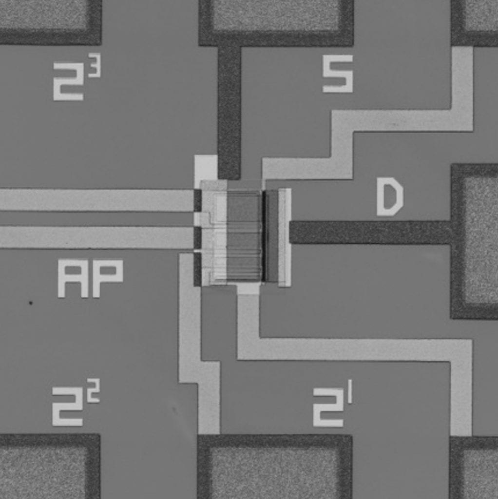
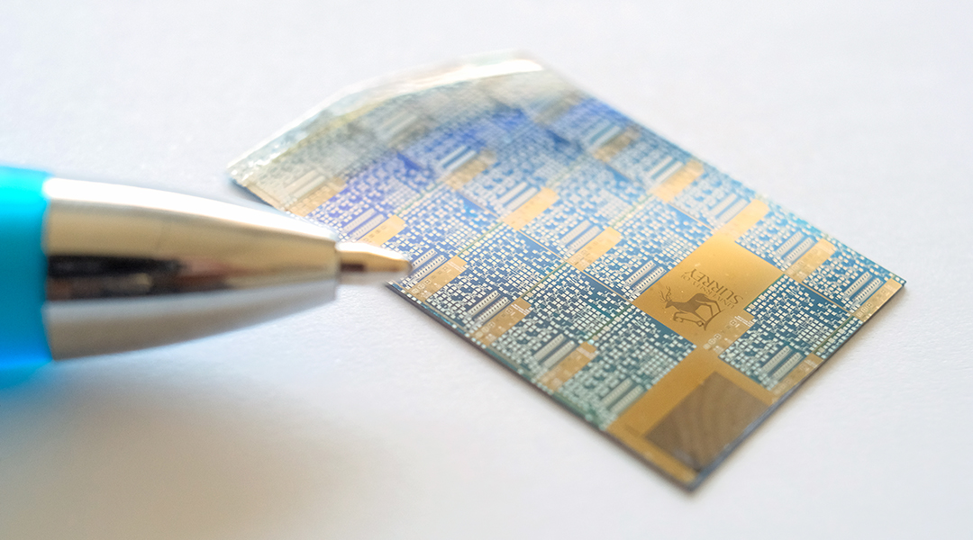
Image credit: Radu Sporea, University of Surrey
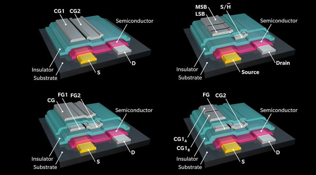
In a study published in Advanced Intelligent Systems, researchers from the University of Surrey and University of Rennes detail how their device, called the multimodal thin-film transistor (MMT), overcomes long-standing challenges and can perform the same operations as more complex circuits.

Thin-film electronic technologies sandwich metals, insulators, and semiconductors in layers that are tens or hundreds of nanometers thick to create functional devices. The cost-effective materials and manufacturing processes are well suited to large-area applications, such as display screens, and, increasingly, to the high-volume fabrication of flexible or printed electronics with applications in well-being, medicine, and environmental monitoring. The main downside of these low-cost techniques is the device-to-device performance variation between transistors, which makes it comparatively difficult to realize large circuits with complex functionality.
Thin-film transistors are used as switches, amplifiers, and current sources. Traditionally, gate electrodes are used to control a transistor’s ability to pass current and the size of the current. In the new device, on/off switching is controlled independently from the amount of current passing through the structure. This allows the MMT to operate at a higher speed than comparable devices and to have a linear dependence between input and output, essential for ultra-compact digital-to-analog conversion. This also gives engineers unprecedented freedom of design, which could lead to greatly simplified circuits, and a much wider range of applications for thin-film, flexible, and printed electronics.
Transistors may also be used as memory devices when designed with “floating gates”. One of the breakthroughs in the recent study is the MMT’s immunity to parasitic effects that reduce a transistor’s capacity to produce uniform, repeatable signals. These have hindered traditional “floating gate” designs ever since their invention in 1967, but this new structure promises efficient analog computation for robotic control, AI and unsupervised machine learning.

This multimodal transistor is a paradigm shift in transistor design. It could change how we create future electronic circuits. Despite its elegantly simple footprint, it has valuable features for processing data from sensors may be the key enabler for future wearables and gadgets beyond the current Internet of Things.
This first demonstration uses the microcrystalline silicon technology perfected at the University of Rennes, owing to its relative maturity and robust process, but the approach is also not restrained to a given material or technology. Here, the basic functionality of the MMT is demonstrated. As long as the right interplay between the constituent layers can be realized, MMTs and circuits should be possible in a wide range of materials. This makes it a truly useful tool for integration with diverse sensor technologies.
Eva Bestelink is the co-inventor of the MMT. She chose to study electronic engineering at the University of Surrey after a career change. Eva said: “The project started tentatively during my BEng, with the idea to create a device based on neural function. Within weeks we had an indication that the transistor’s electrical resilience could be improved by design, but the more we probed, the more useful features we uncovered.”
The project has recently received over £1.1M of research funding from the UK’s Engineering and Physical Sciences Research Council and is set to continue with the demonstration of circuit blocks optimized to the MMTs unique abilities, including low-complexity yet powerful neural network circuits for sensor data classification.
Reference: Radu A. Sporea, et al. Versatile Thin‐Film Transistor with Independent Control of Charge Injection and Transport for Mixed Signal and Analog Computation. Advanced Intelligent Systems (2020). DOI: 10.1002/aisy.202000199


