Advanced Optical Materials Issue 1 is now published, with twelve contributions from leading research groups and covering all aspects of light–matter interactions.
All articles are free to access.
To contribute a paper to the next issue of Advanced Optical Materials, visit http://www.advopticalmat.de/call-for-papers/ .
Sign up to be alerted when the next issue of Advanced Optical Materials is published.
Table of Contents: Advanced Optical Materials, Issue 1
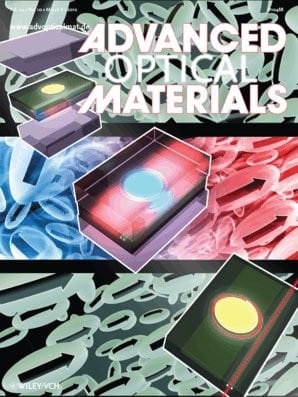
Electro-optical Materials: Efficient Poling of Electro-Optic Polymers in Thin Films and Silicon Slot Waveguides by Detachable Pyroelectric Crystals (Adv. Mater. 10/2012) (page OP1)
Su Huang, Jingdong Luo, Hin-Lap Yip, Ali Ayazi, Xing-Hua Zhou, Michael Gould, Antao Chen, Tom Baehr-Jones, Michael Hochberg and Alex K.-Y. Jen
This first ever Advanced Optical Materialscover design shows a silicon–polymer hybrid slot waveguide ring-resonator modulator being poled by two pyroelectric crystals. Each of the three images, from top to bottom, indicates one stage of the poling—before, during, and after—with the device configuration in the front and the dipole alignment state represented in the background. For details on how this was achieved, check out the article by A. K.-Y. Jen and co-workers on page OP42.
Plasmonics: High Magneto-Optical Activity and Low Optical Losses in Metal-Dielectric Au/Co/Au–SiO2 Magnetoplasmonic Nanodisks (Adv. Mater. 10/2012)(page OP2)
Juan Carlos Banthí, David Meneses-Rodríguez, Fernando García, María Ujué González, Antonio García-Martín, Alfonso Cebollada and Gaspar Armelles
The internal architecture of metal-dielectric Au/Co/Au–SiO2magnetoplasmonic nanodisks provides control over the internal electromagnetic field distribu on by varying the relative contributions of the magneto-optically active layers and the optically lossy layers. This allows simultaneous tuning of the magneto-optical activity and the absorption. On page OP36, A. Cebollada and co-workers show how placing the dielectric between the upper Au layer and the Co produces a configuration of sizeable magneto-optical activity and low optical loss. If the dielectric is placed below the Co, the magneto-optical activity is maintained, but the optical losses are larger.
Editorial: A Bright Future – For Optical Materials (pages OP8–OP9)
Tim Adams and Eva Rittweger
Nanopillars: Large Area Fabrication of Leaning Silicon Nanopillars for Surface Enhanced Raman Spectroscopy (Adv. Mater. 10/2012) (page OP10)
Michael Stenbæk Schmidt, Jörg Hübner and Anja Boisen
M. S. Schmidt et al. describe on page OP11 a simple, two-step fabrication process to as-semble flexible, freestanding nanopillars into large-area substrates. These substrates can be made using readily available silicon-processing equipment and are suitable for SERS, having a large, uniform Raman enhancement.
Large Area Fabrication of Leaning Silicon Nanopillars for Surface Enhanced Raman Spectroscopy (pages OP11–OP18)
Michael Stenbæk Schmidt, Jörg Hübner and Anja Boisen
Giant Optical Gain in a Rare-Earth-Ion-Doped Microstructure (pages OP19–OP22)
Dimitri Geskus, Shanmugam Aravazhi, Sonia M. García-Blanco and Markus Pollnau
A 3D Optical Metamaterial Made by Self-Assembly (pages OP23–OP27)
Silvia Vignolini, Nataliya A. Yufa, Pedro S. Cunha, Stefan Guldin, Ilia Rushkin, Morgan Stefik, Kahyun Hur, Ulrich Wiesner, Jeremy J. Baumberg and Ullrich Steiner
Optical metamaterials have unusual optical characteristics that arise from their periodic nanostructure. Their manufacture requires the assembly of 3D architectures with structure control on the 10-nm length scale. Such a 3D optical metamaterial, based on the replication of a self-assembled block copolymer into gold, is demonstrated. The resulting gold replica has a feature size that is two orders of magnitude smaller than the wavelength of visible light. Its optical signature reveals an archetypal Pendry wire metamaterial with linear and circular dichroism.
Plasmonics: Plasmon-Enhanced Sub-Wavelength Laser Ablation: Plasmonic Nanojets (Adv. Mater. 10/2012) (page OP28)
Ventsislav K. Valev, Denitza Denkova, Xuezhi Zheng, Arseniy I. Kuznetsov, Carsten Reinhardt, Boris N. Chichkov, Gichka Tsutsumanova, Edward J. Osley, Veselin Petkov, Ben De Clercq, Alejandro V. Silhanek, Yogesh Jeyaram, Vladimir Volskiy, Paul A. Warburton, Guy A. E. Vandenbosch, Stoyan Russev, Oleg A. Aktsipetrov, Marcel Ameloot, Victor V. Moshchalkov and Thierry Verbiest
When a droplet hits the surface of water, it is often observed that a water column, or ‘back-jet’, surges upwards. Counterintuitive though it might be, a similar phenomenon can occur when ultrafast light pulses shine on a nanostructured metal surface. These sub-wavelength ‘nanojets’ occur in the regions of highest local field enhancements. For more details, see the article by V. K. Valev et al. on page OP29.
Plasmon-Enhanced Sub-Wavelength Laser Ablation: Plasmonic Nanojets (pages OP29–OP35)
Ventsislav K. Valev, Denitza Denkova, Xuezhi Zheng, Arseniy I. Kuznetsov, Carsten Reinhardt, Boris N. Chichkov, Gichka Tsutsumanova, Edward J. Osley, Veselin Petkov, Ben De Clercq, Alejandro V. Silhanek, Yogesh Jeyaram, Vladimir Volskiy, Paul A. Warburton, Guy A. E. Vandenbosch, Stoyan Russev, Oleg A. Aktsipetrov, Marcel Ameloot, Victor V. Moshchalkov and Thierry Verbiest
In response to the incident light’s electric field, the electron density oscillates in the plasmonic hotspots producing an electric current. Associated Ohmic losses raise the temperature of the material within the plasmonic hotspot above the melting point. A nanojet and nanosphere ejection can then be observed precisely from the plasmonic hotspots.
High Magneto-Optical Activity and Low Optical Losses in Metal-Dielectric Au/Co/Au–SiO2 Magnetoplasmonic Nanodisks (pages OP36–OP41)
Juan Carlos Banthí, David Meneses-Rodríguez, Fernando García, María Ujué González, Antonio García-Martín, Alfonso Cebollada and Gaspar Armelles
Metal-dielectric Au-Co-SiO2magnetoplasmonic nanodisks are found to exhibit large magneto-optical activity and low optical losses. The internal architecture of the nanodisks is such that, in resonant conditions, the electromagnetic field undertakes a particular spatial distribution. This makes it possible to maximize the electromagnetic field at the magneto-optically active layers and minimize it in the other, optically lossy ones.
Efficient Poling of Electro-Optic Polymers in Thin Films and Silicon Slot Waveguides by Detachable Pyroelectric Crystals (pages OP42–OP47)
Su Huang, Jingdong Luo, Hin-Lap Yip, Ali Ayazi, Xing-Hua Zhou, Michael Gould, Antao Chen, Tom Baehr-Jones, Michael Hochberg and Alex K.-Y. Jen
Pyroelectric crystals are used as a conformal and detachable electric field source to efficiently pole electro-optic (E-O) polymers in both parallel-plate (transverse) and in-plane (quasi-longitudinal) configurations. Large Pockels coefficients in poled thin films and high tunability of resonance wavelength shift in hybrid polymer silicon slot waveguide ring-resonator modulators have been achieved using this method.
Photodetection: Spatially Resolved Photodetection in Leaky Ferroelectric BiFeO3(Adv. Mater. 10/2012) (page OP48)
Won-Mo Lee, Ji Ho Sung, Kanghyun Chu, Xavier Moya, Donghun Lee, Cheol-Joo Kim, Neil D. Mathur, S.-W. Cheong, C.-H. Yang and Moon-Ho Jo
On page OP49, M.-H. Jo and co-workers describe a method of control over photocurrent detection by manipulating ferroelectric domain configurations. The magnitude
is spectrally centered around charged domain walls that are associated with oxygen vacancy migration in BiFeO3, where potential gradients caused by spontaneous polarization yield asymmetric and nonlinear photocarrier dynamics.
Spatially Resolved Photodetection in Leaky Ferroelectric BiFeO3 (pages OP49–OP53)
Won-Mo Lee, Ji Ho Sung, Kanghyun Chu, Xavier Moya, Donghun Lee, Cheol-Joo Kim, Neil D. Mathur, S.-W. Cheong, C.-H. Yang and Moon-Ho Jo
Potential gradients due to the spontaneous polarization of BiFeO3 yield asymmetric and nonlinear photocarrier dynamics. Photocurrent direction is determined by local ferroelectric domain orientation, whereas magnitude is spectrally centered around charged domain walls that are associated with oxygen vacancy migration. Photodetection can be electrically controlled by manipulating ferroelectric domain configurations.
Homoepitaxial Growth of Single Crystal Diamond Membranes for Quantum Information Processing (pages OP54–OP59)
Igor Aharonovich, Jonathan C. Lee, Andrew P. Magyar, Bob B. Buckley, Christopher G. Yale, David D. Awschalom and Evelyn L. Hu
Homoepitaxial growth of single crystal diamond membranes is demonstrated employing a microwave plasma chemical vapor deposition technique. The membranes possess excellent structural, optical, and spin properties, which make them suitable for fabrication of optical microcavities for applications in quantum information processing, photonics, spintronics, and sensing.
Self-Assembled Flexible Microlasers (pages OP60–OP64)
Van Duong Ta, Rui Chen and Han Dong Sun
Hemispherical microresonators with tunable sizes are obtained based on the hydrophobic effect on distributed Bragg reflectors. Under optical excitation, whispering gallery mode lasing is observed from the dye-doped microresonators at room temperature. The results indicate the potential application of the flexible microresonators in photonic integrated circuits.
Ultrafast Polymerization Inhibition by Stimulated Emission Depletion for Three-dimensional Nanolithography (pages OP65–OP69)
Joachim Fischer and Martin Wegener
To identify the depletion mechanism in the stimulated-emission-depletion (STED) inspired photoresist composed of a ketocoumarin photoinitiator in pentaerythritol tetraacrylate, we perform lithography with pulsed excitation and tunable delayed depletion. A fast component can unambiguously be assigned to stimulated emission. Our results allow the systematical optimization of the conditions in next-generation STED direct-laser-writing optical lithography.
Graphene: Plasmonic Graphene Transparent Conductors (Adv. Mater. 10/2012)(page OP70)
Guowei Xu, Jianwei Liu, Qian Wang, Rongqing Hui, Zhijun Chen, Victor A. Maroni and Judy Wu
Plasmonic graphene has been fabricated by G. Xu et al. using thermally assisted self-assembly of Ag nanoparticles on graphene. The localized surface-plasmonic effect is demonstrated with the resonance frequency shifting from 446 to 495 nm when the lateral dimension of the Ag nanoparticles increases from about 50 to 150 nm. Both the resonance frequency and amplitude decrease with increasing graphene thickness. In addition, plasmonic graphene shows much improved electrical conductance by a factor of 2–4 as compared to the original graphene.
Plasmonic Graphene Transparent Conductors (pages OP71–OP76)
Guowei Xu, Jianwei Liu, Qian Wang, Rongqing Hui, Zhijun Chen, Victor A. Maroni and Judy Wu
Certain Biominerals in Leaves Function as Light Scatterers (pages OP77–OP83)
Assaf Gal, Vlad Brumfeld, Steve Weiner, Lia Addadi and Dan Oron

