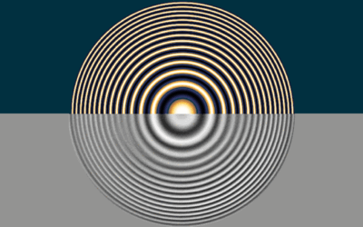
 Advanced Optical Materials Issue 2 is live, with twelve contributions from leading research groups and covering the whole range of light–matter interactions.
All articles are free to access.
To contribute a paper to the next issue of Advanced Optical Materials, visit http://www.advopticalmat.de/call-for-papers/ .
Table of Contents: Advanced Optical Materials, Issue 2
-
Front Cover
-
Youshin Ahn, Eunjoo Kim, Jinho Hyon, Changjoon Kang and Youngjong Kang
Article first published online: 12 JUN 2012 | DOI: 10.1002/adma.201290136
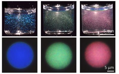
Block copolymer photonic gels exhibiting multiple colors in response to near-UV radiation are demonstrated by Y. Kang and co-workers on page OP 127. The counterions pairing with the polyelectrolyte in the gel layers determine the photosensitivity of photonic gels. The simple replacement of ions can make the photonic gels either highly sensitive or insensitive to near-UV. The illustration shows ionic signaling giving “STOP” and “GO” cues for the photoresponse of these photonic gels.
-
-
Inside Front Cover
-
Xiangming Li, Yucheng Ding, Jinyou Shao, Hongmiao Tian and Hongzhong Liu
Article first published online: 12 JUN 2012 | DOI: 10.1002/adma.201290137
Y. C. Ding, J. Y. Shao, and co-workers demonstrate a creative and economic method for manufacturing large-area microlens arrays (MLAs) with controllable curvature and supersmooth surfaces. On page OP 165, the production of a concave MLA is achieved by electrohydrodynamically deforming the surface of a photocurable prepolymer trapped in microhole array which has been etched onto a doped silicon wafer. The concave MLA is then used as a master to generate the convex MLA via vacuum micromoulding.
-
-
Back Cover
-
Metamaterial Electromagnetic Wave Absorbers (Adv. Mater. 23/2012) (page OP181)
Claire M. Watts, Xianliang Liu and Willie J. Padilla
Article first published online: 12 JUN 2012 | DOI: 10.1002/adma.201290138
-
-
Editorial
-
Metamaterials Top the Advanced Materials Charts (page OP97)
Article first published online: 12 JUN 2012 | DOI: 10.1002/adma.201290141
-
-
Progress Report
-
Metamaterial Electromagnetic Wave Absorbers (pages OP98–OP120)
Claire M. Watts, Xianliang Liu and Willie J. Padilla
Article first published online: 25 MAY 2012 | DOI: 10.1002/adma.201200674
-
-
Frontispiece
-
Shingo Araki, Kazuki Nakamura, Kanae Kobayashi, Ayako Tsuboi and Norihisa Kobayashi
Article first published online: 12 JUN 2012 | DOI: 10.1002/adma.201290142
A novel electrochromic device with three optical states – transparent, specular mirror, and black – is demonstrated by N. Kobayashi and co-workers on page OP 122. The cell i
s constructed by sandwiching gel electrolyte-containing silver nitrate between one flat and one particle-modified in-dium thin oxide electrode. The optical states can be switched by altering the potential across the two electrodes.
-
-
Communications
-
Shingo Araki, Kazuki Nakamura, Kanae Kobayashi, Ayako Tsuboi and Norihisa Kobayashi
Article first published online: 10 MAY 2012 | DOI: 10.1002/adma.201200060
A novel electrochromic device with three optical states, transparent, specular mirror, and black, is demonstrated. The cell is constructed by sandwiching gel electrolyte containing silver nitrate between one flat and one particle-modified indium thin oxide electrode. The optical states can be switched by altering the potential across the two electrodes. All changes are reversible and show good stability over 2500 cycles of testing.
-
Youshin Ahn, Eunjoo Kim, Jinho Hyon, Changjoon Kang and Youngjong Kang
Article first published online: 10 FEB 2012 | DOI: 10.1002/adma.201103767
Block copolymer photonic crystalscomprising polyelectrolyte hydrogels exhibit strong reflective multicolors in response to near-UV radiation. Due to unique volume transition of swollen gels, the photonic gels show high photosensitivity, and which can be widely tunable by exchanging counter-anions. Multicolor photonic patterns created by photolithography can be repeatedly fixated and reactivated by sequentially exchanging counter-anions with different photosensitivity.
-
Yan Jun Liu, Guang Yuan Si, Eunice S. P. Leong, Ning Xiang, Aaron J. Danner and Jing Hua Teng
Article first published online: 21 MAR 2012 | DOI: 10.1002/adma.201104440
Light-driven plasmonic color filters are demonstrated by integrating gold annular aperture arrays with photoresponsive liquid crystals (LCs). Upon photoirradiation, a nematic−isotropic phase transition of the LCs arises from the trans–cisphotoisomerization of photochromic LCs. As a consequence, the effective refractive index experienced by the impinging light changes, modulating the transmission intensity.
-
Metal–Polymer–Metal Split-Dipole Nanoantennas (pages OP136–OP142)
Deirdre M. O’Carroll, James S. Fakonas, Dennis M. Callahan, Martin Schierhorn and Harry A. Atwater
Article first published online: 22 MAR 2012 | DOI: 10.1002/adma.201103396
The conjugated polymer semiconductor poly(3-hexylthiophene), (P3HT), is integrated directly into the slot region of resonant plasmonic split-dipole nanoantennas. The P3HT radiative emission rate is enhanced by a factor of up to 29, in experiment, and 550 for the ideal case, due to the large local density of optical states in the nanoantenna slot region. Additionally, the theoretical modified luminescence quantum efficiency is shown to increase from 1% to 45% for optimized nanoantenna parameters.
-
Chen Zaichun, Mohsen Rahmani, Gong Yandong, Chong Tow Chong and Hong Minghui
Article first published online: 22 MAR 2012 | DOI: 10.1002/adma.201104575
A three-dimensional metamaterial tube is fabricated by rolling up 2D metamaterials on flexible PEN substrate. This novel 3D design of metamaterials can be used to effectively tune the resonance frequency by varying its diameter. Meanwhile, it can also be applied in material identification with a solid-core metamaterials tube.
-
Yueh-Chun Lai, Hsin-Cheng Lee, Shu-Wen Kuo, Cheng-Kuang Chen, Hsieh-Ting Wu, Oscar K. Lee and Ta-Jen Yen
Article first published online: 15 MAY 2012 | DOI: 10.1002/adma.201200291
Intracellular imaging by exciting multimode resonances in spilt-ring resonators (SRRs) is presented. With advantages such as being label-free, coupler-free, having a tunable spectrum range and in
tracellular detection length, SRR microscopy is a strong competitor for surface plasmon resonance microscopy for observing cells. Its capability for constructing refractive index distribution images of cells is demonstrated. SRR microscopy offers a much simpler optical configuration and better penetration depth for truly whole-cell imaging applications.
-
Hailong Ning, Agustin Mihi, Joseph B. Geddes III, Masao Miyake and Paul V. Braun
Article first published online: 9 MAY 2012 | DOI: 10.1002/adma.201104769
The photonic density of states (DOS) of a silicon inverse photonic crystal is probed using the radiative emission of LaF3:Nd nanoparticles. These emitters are embedded as a thin planar defect within the interior of photonic crystals with varying silicon filling fractions. The alignment of the narrow emission of the particles with the high and low photonic DOS regions is achieved. The time-resolved measurements reveal that the radiative lifetime of the embedded Nd3+ is strongly influenced by the surrounding DOS provided by the silicon inverse opals.
-
Yile Liao, Guichuan Xing, Nimai Mishra, Tze Chien Sum and Yinthai Chan
Article first published online: 18 MAY 2012 | DOI: 10.1002/adma.201200121
Wet-chemically synthesized CdSe seeded CdS nanotetrapods incorporated into silica matrices have been explored as high performance nanocrystal-based optical amplifiers. Varying the physical dimensions of the tetrapods allowed for room temperature biexcitonic amplified spontaneous emission (ASE) at wavelengths corresponding to either the CdSe core or CdS arms, while higher pump intensities resulted in ASE from a higher CdSe excited state. These results collectively indicate that such heterostructured tetrapods can facilitate tunable, multiple-wavelength lasing across a wide spectral range from a single nanostructure.
-
Xiangming Li, Yucheng Ding, Jinyou Shao, Hongmiao Tian and Hongzhong Liu
Article first published online: 22 MAR 2012 | DOI: 10.1002/adma.201104625
The microlens array (MLA) or micromirror array (MMA) is one of the most important units in many optical devices and photoelectronic systems. The paper presents a process for fabricating an MLA with well-controlled curvature by liquid trapping and electrohydrodynamic deformation in microholes. The approach has been shown capable of generating large-area and high-quality MLAs or MMAs economically.
-
Can Nanotubes Make a Lens Array? (pages OP170–OP173)
Ranjith Rajasekharan, Haider Butt, Qing Dai, Timothy D. Wilkinson and Gehan A. J. Amaratunga
Article first published online: 9 MAY 2012 | DOI: 10.1002/adma.201200296
Reflective binary Fresnel lenses fabricated so far all suffer from reflections from the opaque zones and hence degradation in focusing and lensing properties. Here a solution is found to this problem by developing a carbon nanotube Fresnel lens, where the darkest man-made material ever, i.e., low-density vertically aligned carbon nanotube arrays, are exploited.
-
-
Frontispiece
-
Pola Goldberg-Oppenheimer, Sumeet Mahajan and Ullrich Steiner
Article first published online: 12 JUN 2012 | DOI: 10.1002/adma.201290143
On page OP 175, U. Steiner and co-workers destabilise polymer trilayer films using an electric field to generate separated micrometre-sized core-shell pillars, which are further modified by selective polymer dissolution to yield polymer core columns surrounded by a rim and micro-volcano rim structures. When coated with gold and decorated with Raman active probes, all three structure types give rise to substantial enhancement in surface-enhanced Raman scattering (SERS). Since this SERS enhancement arises from each of the isolated structures in the array, these surface patterns are an ideal platform for multiplexed SERS detection.
-
-
Full Paper
-
Pola Goldberg-Oppenheimer, Sumeet Mahajan and Ullrich Steiner
Article first published online: 4 APR 2012 | DOI: 10.1002/adma.201104159
Electrohydrodynamic (EHD) instabilities are employed to create hierarchical structures including, pillars, coaxial morphologies and rims with sub-micrometer edges, which are further used as substrates for surface-enhanced Raman scattering (SERS). 1.0 × 10⁷ SERS enhancements from isolated rims and coaxial patterns are observed. Since SERS enhancement arises from each of the isolated structures in the array, EHD-patterned substrates provide optimal platforms for high-throughput SERS detection, where each of the individual EHD structures can be used to detect a different molecular component.
-

