In today’s day and age, most of the world’s population carries “technology in hand”, be it in the form of smartphones, laptops, tablets or smart watches. This is the outcome of integrated miniaturized electronic circuits made of billions of building blocks like transistors.
Two dimensional (2D) materials are atomically thin layered materials, which demonstrate exceptional electronic transport properties compared to bulk materials, and may be potential candidates for future transistor technology. Graphene is one of the most explored 2D materials today, and consists of a monolayer of carbon atoms arranged in a honeycomb lattice crystal structure. When two atomically thin monolayers of graphene are stacked, the inter-layer interaction typically results in modifications of electronic properties.
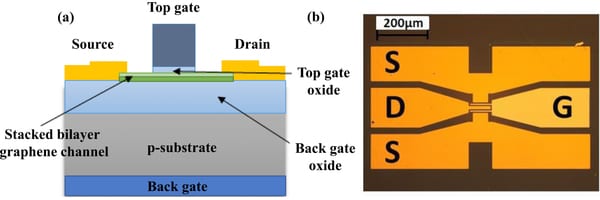
In recently published research, researchers from Germany, France and Spain report performance enhancement in individual field effect transistors (FETs) fabricated using artificially stacked graphene double-layers (bilayers), and compare these with similar transistors from single layer graphene. In general, the conductance in the output response is lowered in these stacked bilayer graphene FETs, which leads to an improved intrinsic voltage gain performance. This implies improved signal amplification by the stacked bilayer transistors, when compared to monolayer graphene transistors.
The authors suggest that these observations may attribute to a higher field induced carrier density in artificially stacked bilayer graphene devices. Such enhancement in transistor performance may propel future applications of large area graphene layers in areas like telecommunication, radar and large area display technologies.
Text kindly provided by the Authors.


