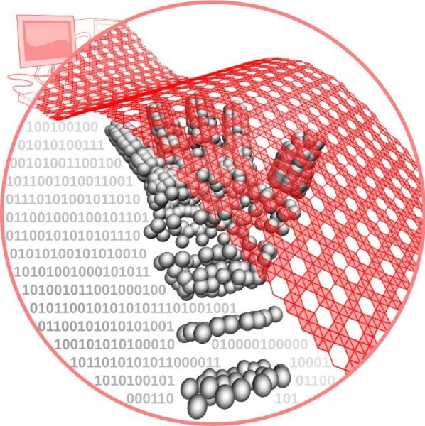
Two-dimensional sheets of boron that can be lifted off a substrate are possible to make via several theoretical methods suggested in a new paper by Rice University scientists. The material could be a useful complement to graphene and other 2-D materials for electronics, they said. Image: Evgeni Penev/Rice University.
It would be a terrible thing if laboratories striving to grow graphene from carbon atoms kept winding up with big pesky diamonds.
“That would be trouble, cleaning out the diamonds so you could do some real work,” said Rice University theoretical physicist Boris Yakobson, chuckling at the absurd image.
Yet something like that keeps happening to experimentalists working to grow two-dimensional boron. Boron atoms have a strong preference to clump into three-dimensional shapes rather than assemble into pristine single-atom sheets, like carbon does when it becomes graphene. And boron clumps aren’t nearly as sparkly.
Yakobson and his Rice colleagues have made progress toward 2-D boron through theoretical work that suggests the most practical ways to make the material and put it to work. Earlier calculations by the group indicated 2-D born would conduct electricity better than graphene.
Through first-principle calculations of the interaction of boron atoms with various substrates, the team came up with several possible paths experimentalists may take toward 2-D boron. Yakobson feels the work may point the way toward other useful two-dimensional materials.
Yakobson’s lab first reported in a Nano Letters paper last year that unlike graphene, 2-D boron rolled into a nanotube would always be metallic. Also unlike graphene, the atomic arrangement can change without changing the nature of the material. Instead of the steady rank-and-file of hexagons in a perfect graphene sheet, 2-D boron consists of triangles. But boron could have vacancies – missing atoms – without affecting its properties.
That’s the theory. The problem that remains is how to make the stuff.
“We are, perhaps, so close,” Penev said. “Here we have conceived a material that resembles graphene, but is always conductive no matter what form it takes. What we’re doing now is exploring different possibilities to connect our theories with reality.”
The best method, they calculated, might be to feed boron into a furnace with silver or gold substrates in a process called chemical vapor deposition, commonly used to make graphene. The substrate is important, Penev said, because the atoms have to spill onto the surface and stick, but not too strongly.
“You have to have a substrate that doesn’t want to dissolve boron,” he said. “On the other hand, you want a substrate that doesn’t bind too strongly. You should be able to detach the boron layer.”
Then, like graphene, these atom-thick boron sheets could be applied to other surfaces for testing and, ultimately, for use in applications.
The study also calculated methods for creating sheets via saturation of boron atoms on the surface of boride substrates, and the evaporation of metal atoms from metal borides that leaves just the target atoms in a sheet.
“There are a lot of reasons boron could be interesting,” said Liu, the paper’s first author. “Boron is carbon’s neighbor on the periodic table, with one less electron, which might bring in lots of new physics and chemistry, especially on the nanoscale. For example, 2-D boron is more conductive than graphene because of its unique electronic structure and atomic arrangement.
“In fact, comparing (boron) with graphene is very helpful,” he said. “The state-of-art synthesis methods for graphene provide us good templates to explore 2-D boron synthesis.”
Yakobson is thinking a step beyond the current work. “There are many groups, at Rice and elsewhere, working on 2-D boron,” he said. “To appreciate this work, you have to stand back and contrast it with graphene; in some sense, the synthesis of graphene is trivial.
“Why? Because graphene is a God-given material,” he said. “It forms at the global minimum (energy) for carbon atoms – they go there willingly. But boron is a different story. It does not have a planar form as a global minimum, which makes it a really subtle problem. The novelty in this work is that we’re trying to trick it into building a two-dimensional motif instead of three.”
The search for 2-D materials with varying qualities is hot right now; another new paper from Rice on a hybrid graphene-hexagonal boron nitride shows the need for a 2-D semiconductor to complement the material’s conducting and insulating elements.
Yakobson hopes his study serves as a guideline for practical routes to other novel materials. “Now that there is a growing interest in a variety of 2-D materials, this may be a template,” he said.
Source: Rice University


