A strategy for placing bezel-less image sensors for electronic devices over the entire surface of a tetrahedral, 3D sensor is demonstrated.
![Transforming Planar Electronic Devices into 3D Structures [Video]](https://www.advancedsciencenews.com/wp-content/uploads/2018/07/adma201801256_ASN-image_smaller.png)
A strategy for placing bezel-less image sensors for electronic devices over the entire surface of a tetrahedral, 3D sensor is demonstrated.
Wearable electronic device can be inserted into convential wound dressings.
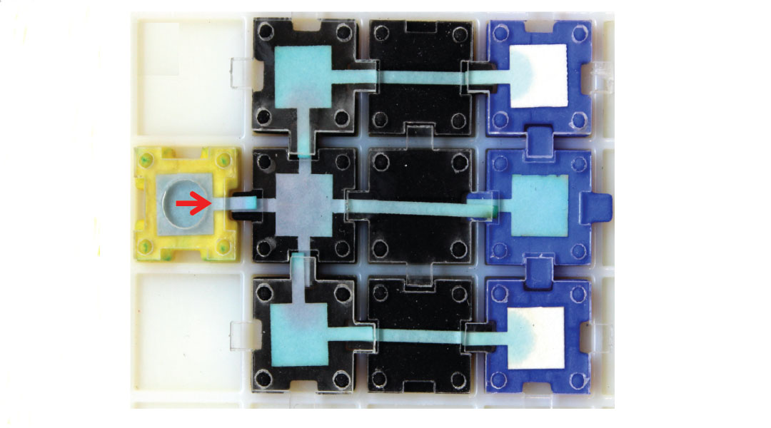
A team of researchers construct a library of pre-fabricated, reusable paperfluidic blocks for point-of-care diagnostic devices.

American researchers designed a smartphone octo‐channel optosensor (SOS) for low‐cost low‐volume lab tests as a mHealth diagnostic tool.
Disposable and flexible electronics made from paper could provide a cost-effective alternate to current electronic device materials.
![Unravelling the Cytokine Secretion Process of Single Cells with a Novel Biosensor [Video]](https://www.advancedsciencenews.com/wp-content/uploads/2018/07/smll201800698_ASN_image_3.jpg)
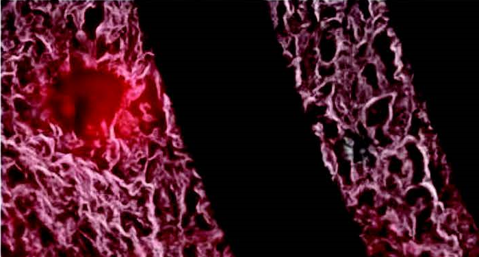
A nanobiosensor is developed that performs real-time analysis of single-cell cytokine secretion, enabling the development of new therapies for diseases.
![A Dual-Modal Probe for Early Detection of Alzheimer’s Disease [Video]](https://www.advancedsciencenews.com/wp-content/uploads/2018/06/smll201800901_ASN_image.jpg)
A novel probe for imaging amyloid-β (Aβ) in vivo is developed, enabling the early detection and diagnosis of Alzheimer’s disease.
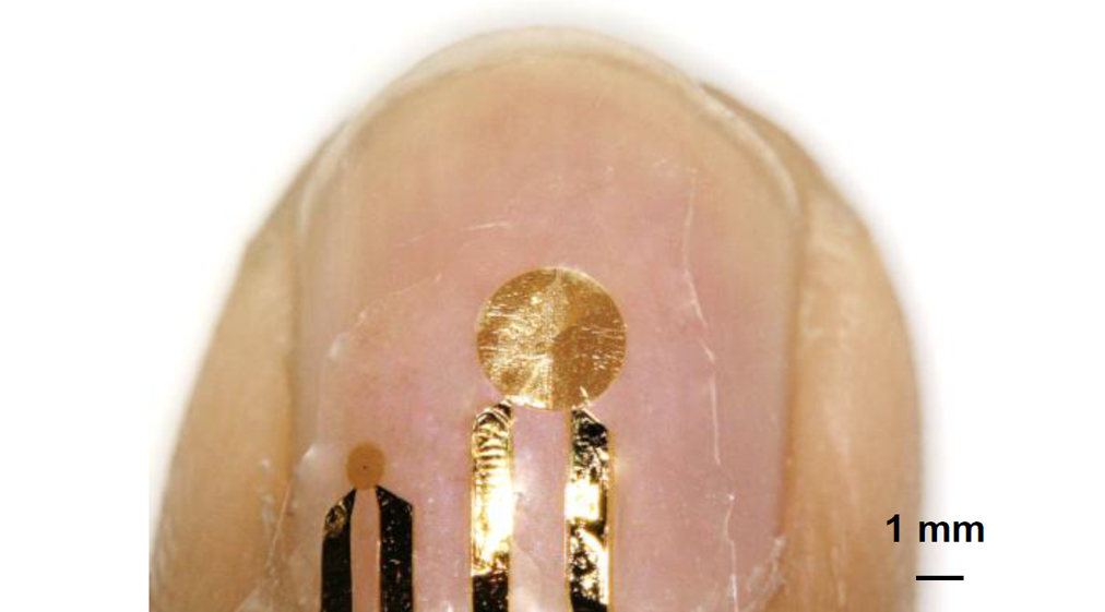
A wearable fingernail sensor that can collect thermal data of the nailbed tissue in real-time is developed.
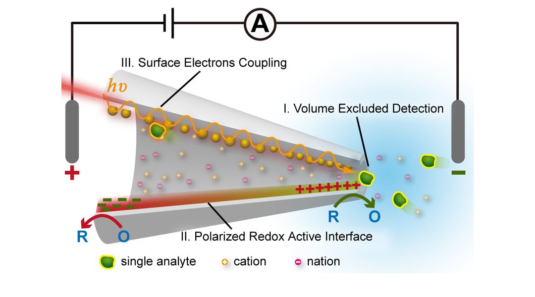
Electrochemical confined effects are capable of exploring the novel detection mechanisms of nanopore to efficiently convert the dynamic function/structure of single molecules into the ionic signatures or optical patterns. This will prompt the nanopore to emerge on the comprehensive range of future applications in both life and material science.
![Super-Repellent Surfaces Based on Triply Re‐Entrant Structures [Video]](https://www.advancedsciencenews.com/wp-content/uploads/2018/05/adma201800103_ASN_image_003.jpg)
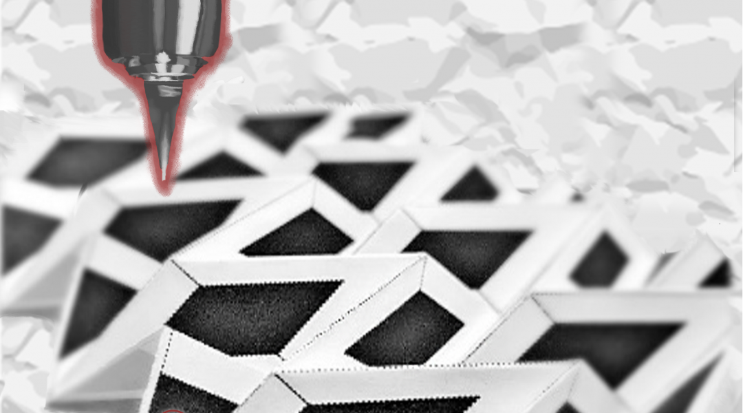
Zhongze Gu and colleagues from Southeast University in China utilize direct laser writing to 3D-print omniphobic, triply re-entrant surfaces that can universally repel organic liquids.
 New theory suggests gravity is not a fundamental force
 Quantum entanglement visualized for the first time ever
 Scientists take a closer look at rare particles called hypernuclei
 French WEST reactor breaks record in nuclear fusion
 Higgs boson may be driving the Universe’s expansion
 Researchers take a glimpse at the structure of rare tetraquarks
 Black hole images deliver a deathblow to alternative theory of gravity
 An anti-inflammatory peptide may hold the key to low-back pain relief
 CERN scientists search for new physics in unusual energy patterns linked to hidden particles
 String theory provides a new take on the expansion of the Universe