 The exceptional properties of diamond, including a wide electronic and optical band gap, excellent thermal conductivity, and its biocompatibility, make this material highly attractive for numerous applications. In the field of quantum computing a specific diamond color center, the negatively charged nitrogen vacancy center, is one of most promising solid state qubits due to its room temperature operation, long spin coherence time, and suitability for optical initialization and readout. However, great challenges remain in the fabrication of thin diamond membranes, which are necessary for planar photonic device engineering.
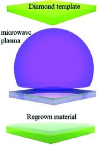
Igor Aharonovich and co-workers (Harvard University) have now demonstrated an innovative approach to engineer nanometer thick diamond slabs. They used chemical vapor deposition to epitaxially grow high quality, nanometer thick diamond membranes on top of ion-damaged diamond templates. The overgrown material exhibits bright luminescence, excellent Raman signature and good spin coherence times associated with the nitrogen vacancy (NV) defect. Moreover, by modifying the growth conditions, incorporation of different emitters into the diamond membrane could be controlled. Microdisk cavities with quality factors approaching ~ 3000 prove the suitability of the new material for quantum applications.
This technological breakthrough enables the formation of free standing, high quality diamond membranes and offers a scalable approach for diamond device fabrication for a variety of applications.
The research is reported in the first issue of Advanced Optical Materials, the new section in Advanced Materials dedicated to exploring light-matter interactions. The paper, “Homoepitaxial Growth of Single Crystal Diamond Membranes for Quantum Information Processing“, is available for free download now!


