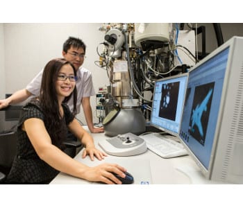
Haimei Zheng and Hong-Gang Liao used TEMs at the National Center for Electron Microscopy and a K2-IS camera to record the first direct observations of facet formation in platinum nanocubes. Photo by Kelly Owen.
The first direct observations of how facets form and develop on platinum nanocubes point the way towards more sophisticated and effective nanocrystal design and reveal that a nearly 150 year-old scientific law describing crystal growth breaks down at the nanoscale.
Researchers with the U.S. Department of Energy (DOE)’s Lawrence Berkeley National Laboratory (Berkeley Lab) used highly sophisticated transmission electron microscopes and an advanced high-resolution, fast-detection camera to capture the physical mechanisms that control the evolution of facets – flat faces – on the surfaces of platinum nanocubes formed in liquids. Understanding how facets develop on a nanocrystal is critical to controlling the crystal’s geometric shape, which in turn is critical to controlling the crystal’s chemical and electronic properties.
“For years, predictions of the equilibrium shape of a nanocrystal have been based on the surface energy minimization proposal by Josiah Willard Gibbs in the 1870s to describe the equilibrium shape of a water droplet,” says Haimei Zheng, a staff scientist in Berkeley Lab’s Materials Sciences Division who led this study. “For nanocrystals, the idea is that during crystal growth, high-energy facets will grow at a higher rate than low-energy facets and eventually disappear, resulting in a nanocrystal whose shape is configured to minimize surface energy.”
The research of Zheng and her collaborators showed that at the molecular level, the geometric shape of nanocrystals during synthesis in solution is actually driven by differences in the mobility of ligands across the surfaces of different facets.
“By choosing ligands that selectively bind on the facets, we should be able to control the shape of the nanocrystal as it grows,” she says. “This would provide a new way to design nanomaterials for advanced applications, including nanostructures for bio-imaging, catalysts for solar conversion, and energy storage.”
Zheng is the corresponding author of a paper in Science titled “Facet Development During Platinum Nanocube Growth.” Hong-Gang Liao is the lead author. Co-authors are Danylo Zherebetskyy, Huolin Xin, Cory Czarnik, Peter Ercius, Hans Elmlund, Ming Pan and Lin-Wang Wang.
The performance of nanocrystals in such surface-enhanced applications as catalysis, sensing and photo-optics is strongly influenced by shape. While significant advances have been made in the synthesis of nanocrystals featuring a variety of shapes – cube, octahedron, tetrahedron, decahedron, icosahedron, etc., – controlling these shapes is often difficult and unpredictable.
“A major roadblock has been that the atomic pathways of facet development in nanocrystals are mostly unknown due to the lack of direct observation,” Zheng says. “It has been assumed that commonly used surfactants modify the energy of specific facets through preferential adsorption, thereby influencing the relative growth rate of different facets and the shape of the final nanocrystal. However, this assumption was based on post-reaction characterizations that did not account for how facet dynamics evolve during crystal growth.”
As a crystal undergoes growth, its constituent atoms or molecules fan out along specific directional planes whose coordinates are denoted by a three-digit system called the Miller Index. Facets form when the surfaces along different planes grow at different rates. Three of the most critical facets for determining a crystal’s geometric shape are the so-called “low index facets,” which are designated under the Miller Index as {100}, {110} and {111}.
Working with platinum, one of the most effective industrial catalysts in use today, Zheng and her collaborators initiated the growth of nanocubes in a thin layer of liquid sandwiched between two silicon nitride membranes. This microfabricated liquid cell can encapsulate and maintain the liquid inside the high vacuum of a transmission electron microscope (TEM) for an extended period of time, enabling in situ observations of single nanoparticle growth trajectories.

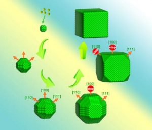
Berkeley Lab researchers found that differences in ligand mobility during crystallization cause the low index facets – {100}, {110} and {111} – to stop growing at different times, resulting in the crystal’s final cubic shape. Image courtesy of Haimei Zheng group.
“With the liquid cells, we’re able to use TEMs to observe the growth of nanocrystals that remarkably resemble nanocrystals synthesized in flasks,” Zheng says. “We found that the growth rates of all low index facets are similar until the {100} facets stop growing. The {110} facets will continue to grow until they reach two neighboring {100} facets, at which point they form the edge of a cube whose corners will be filled in by the continued growth of {111} facets. The arrested growth of the {100} facets that triggers this process is determined by ligand mobility on the {100} facets, which is much lower than on the {110} and {111} facets.”
For their observations, Zeng and her collaborators were able to use several of the TEMs at Berkeley Lab’s National Center for Electron Microscopy (NCEM), a DOE Office of Science user facility, including the TEAM 0.5 instrument, the world’s most powerful TEM. In addition, they were able to use a K2-IS camera from Gatan, Inc., which can capture electron images directly onto a CMOS sensor at 400 frames per second (fps) with 2K-by-2K pixel resolution.
“The K2-IS camera can also be configured to capture images at up to 1600 fps with appropriate scaling of the field of view, which is critical for observing particles that are moving dynamically in the field of view,” says lead author Liao, a member of Zheng’s research group. “The elimination of the traditional scintillation process during image detection results in significant improvement in both sensitivity and resolution. High resolution imaging is also facilitated by the thin silicon nitride membranes of our liquid cell window, which is about 10 nanometers thick per membrane.”
The lower ligand mobility and arrested growth of selected facets experimentally observed by Zheng and Liao, were supported by ab initio calculations carried out under the leadership of co-author Wang, a senior scientist with the Materials Sciences Division who heads the Computational Material Science and Nano Science group.
“At first, we thought the continued growth in the {111} direction might be a result of higher surface energy on the {111} plane,” says co-author Zherebetskyy, a member of Wang’s group. “The experimental observations forced us to consider alternative mechanisms and our calculations show that the relatively low energy barrier on the {111} plane allow the ligand molecules on that plane to be very mobile.”
Says Wang, “Our collaboration with Haimei Zheng’s group showcases how ab initio calculations can be combined with experimental observations to shed new light on hidden molecular processes.”
Zheng and her group are now in the process of determining whether the ligand mobility in platinum that shaped the formation of cube-shaped nanocrystals also applies to ligands in other nanomaterials and the formation of nanocrystals in other geometric shapes.
Source: Berkeley Lab


