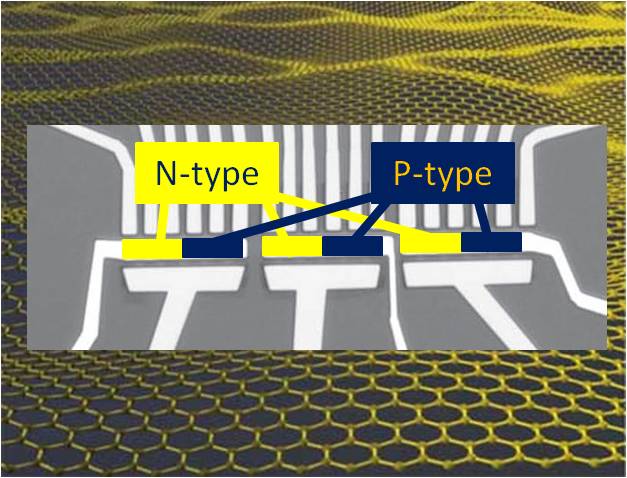
New work now demonstrates that the use of lithographically prepared bilayer graphene (BLG) transistors in logic gates is feasible when following a modified self-adaptive architecture.
Miniaturization and power optimization are hot topics in microelectronics, with special focus on building next generation logic devices. Replacing current silicon-based complementary metal-oxide semiconductor (CMOS) technology requires a material to have high carrier mobility and short scaling length. Graphene has been hailed as such a candidate. New work now demonstrates that the use of lithographically prepared bilayer graphene (BLG) transistors in logic gates is feasible when following a modified self-adaptive architecture.
BLG transistors are inherently ambipolar, making them unsuitable for logic development, but through the use of charge neutrality points (CNPs) inherent to graphene, the transistors can be switched between n- and p-type. This switchability/self-adaptability is achieved through the use of a supply bias (VDD). To enhance this process, an electrostatic doping modulation is introduced via an added dielectric layer, a technique that seems less invasive than doping. The addition of this layer is easily done the current fabrication technologies. With the use of this modified architecture, the transistors show switchability at much lower VDD values.
The devises are tested firstly in a simple NOT gate consisting of a complementary pair of transistors. Parameters including voltage gain and output swing are the most interesting, especially in a regime where VDD is kept below 1V (low power regime). A rise in the performance is marked, with an output swing of up to 90%, and it is stated that with added band-gap engineering the switching ratio can be improved. More complex NAND and NOR gates are also demonstrated for the first time using graphene, illustrating the feasibility of this technique in preparing logic devices.


