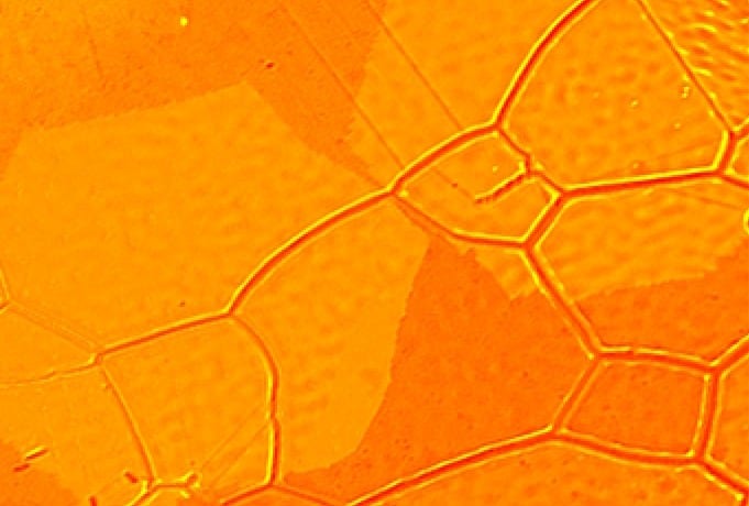
 Graphene is a two-dimensional crystal with extremely high carrier mobility. Techniques are available to synthesize wafer-scale graphene film, but the wafers are polycrystalline with typical grain size of tens of microns or smaller. The grain boundaries degrade material performances. Therefore, it is very important to develop strategy to enlarge the grain size.
Now, a Chinese research group have developed a new process which enables synthesis of graphene grains up to ~1.2 mm, the largest on a Cu substrate. The researchers used polystyrene as solid carbon source because of its relative weak C-H bonds compared to common gaseous sources.Process optimization enabled a nucleation density as low as ~100 nuclei/cm2, and continuous increase in carbon supply and the gas flow rate drives continuous growth. The graphene grains show high crystalline quality with high mobility of 5000-8000 cm2V-1s-1. The researchers are confident that their work will benefit application of graphene in electronics.


