Counterfeit goods are a prevalent global issue, often having a detrimental impact on a country’s economy. “Knock-offs” may look and feel like the real thing, but in reality, counterfeit products are often under-performing, lower quality versions of the item they are trying to replicate. In some cases, even being dangerous to the user.
Anticounterfeiting technologies are therefore highly sought after. The main challenge is to create a technology that is difficult, or even impossible to replicate, while being fast and simple to reproduce.
Nanocrystal inks, consisting of nanoparticles having multiple shapes and sizes, could be a promising solution. These would allow for high-resolution, controllable patterns to be printed in a matter of seconds.
To make such inks, a simple one-step process has been revealed.
A light pattern is projected on a photoconductor/Cu2+ electrolyte interface, removing the kinetic barrier needed for discharging metal ions and causing the photoelectrochemical reduction of Cu2+ to Cu2O nanocrystals on the defined area. By simultaneously fine-tuning the light wavelength, photoconductor thickness, and light intensity, the Cu2+ reduction process can be controlled.
The sharpness of the projected pattern can also be adjusted by varying the amount of charge transferred during electrodeposition; and by carefully controlling the light intensity, charge density, and applied potential, the nanoparticle size, density, and shape can be regulated.
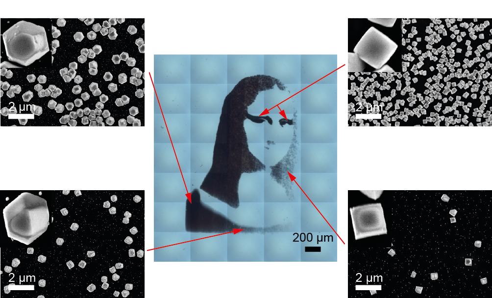
Hidden cryptic polyhedral signature.
Using this facile printing method, micrometer-scale patterns with multiple levels of security can be produced. To the end user, the patterns are identifiable using a generic optical microscope; while more specialized analysis with an electron microscope reveals hidden nanocrystal signatures.

