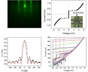
For more information about this figure, please refer to the original journal article here.
Magnesium diboride (MgB2) is a promising superconducting material, with a critical temperature Tc of 39 K – the highest among conventional superconductors at ambient pressure. This high Tc allows MgB2 based superconducting electronics, such as Josephson junctions and superconducting quantum interference devices (SQUID), to operate at relatively higher temperatures (≥ 20 K) and higher speeds. MgB2 has a hexagonal layered crystal structure and is readily coupled with many other layered hexagonal materials, such as graphene, transition-metal dichalcogenides, and many topological insulators, to build novel devices for information sensing and processing.
To create epitaxial MgB2 films suitable for mass production, molecular beam epitaxy (MBE) is the most proper growth technique. It can enable one step growth of epitaxial MgB2 films at relatively low substrate temperature (150–320 °C, suitable for multilayer growth and subsequent device integration). However, even within such a narrow temperature window, the ability to control the film quality is a delicate process. With help of in situ reflection high-energy electron diffraction (RHEED) patterns, the research group at University of Waterloo led by Prof. Guo-Xing Miao recently found a way to grow high quality MgB2 films on whole Si wafers by adopting a self-limiting growth process. The team also fabricated micro-sized MgB2/MgO/MgB2 Josephson junctions. Transport measurements on these junctions exhibit very good I-V characteristics. Field modulations of the I–V curves show clear Fraunhofer patterns and Fiske steps, further confirming extremely good quality of the materials . These achievements pave the way for large-scale deployment of MgB2 thin film devices.


