 UK scientists develop method to produce and identify boron nitride monolayers like graphene using simple laboratory techniques.
Everyone is now familiar with graphene, the atomically thick layer of carbon atoms, for which Andre Geim and Konstantin Novoselov won the 2010 Nobel Prize for Physics. But what about other atomic monolayers with interesting properties?
Boron nitride (BN) has been attracting some recent interest. It is isoelectronic with graphene and shares some of the same properties, but also potentially has many different and exciting ones; for example, it is an insulator whereas graphene can conduct. However studying thin layers of BN has been difficult until now, because they could not be made in the same easy way as layers of graphene. Identifying the monolayers of BN is also harder than for graphene, as BN does not absorb visible light.
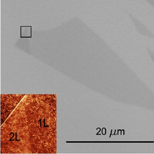
A recent paper from the group of Geim and Novoselov at University of Manchester, UK, demonstrates a micromechanical cleavage procedure on an oxidized silicon wafer. The scientists use the method on tiny crystals of hexagonally arranged BN to produce atomically thin layers the size of the crystals themselves, much larger than any previously produced. They also demonstrate a smart method to inspect the produced sheets using Raman spectroscopy to easily identify which are monolayers and bilayers. Each additional layer gives rise to a steplike shift in the Raman spectrum.
Because the BN sheets could now be as large as graphene sheets, it should be possible to use them in electronic applications alongside graphene to make very thin components. Importantly, this new method means that monolayer BN can now be studied in depth to determine its properties and see where it can best be used.


