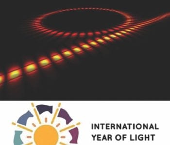
2015 was the International Year of Light, proclaimed by the United Nations to recognize the achievements of light science and its applications, and its contributions to humankind. It raised special attention for major topics and key technologies in the field of optics and photonics. Advanced Optical Materials contributed to this goal by publishing a special series of outstanding review articles.
 For data transmission, optical signals have the advantage to provide high data transfer rates. Therefore, it would be highly desirable to include optical transmission technology into electronic circuits to boost data transfer rates between and within electronic chips. However, the integration of optical data circuits into existing electronic chips has a problem of size mismatch. Due to the diffraction of light the optical signal cannot be localized to less than a few hundred nanometers, whereas modern electronic chips measure only tens of nanometers. The solution to this problem lies in the design of photonic components based on metallic nanostructures, the so-called plasmonic components, which can trap the optical field by coupling it to free-electron excitations near a metal surface on length scales comparable to the sizes of electronic interconnects.
In their comprehensive review article, Alexey Krasavin and Anatoly Zayats (King’s College London) summarize recent advances in the development of active and passive nanophotonic components based on dielectric-loaded plasmonic waveguides. Dielectric-loaded surface plasmon polariton waveguides (DLSPPWs) are of particular interest for applications due to their integrated active functionalities. This includes active control of plasmonic propagation using thermo-optic, electro-optic, and all-optical switching, as well as compensation of propagation losses. The principles and performance of such waveguides are discussed and the current status of the related active plasmonic components that can be integrated in silicon or other nanophotonic circuitries is summarized. Furthermore, a comparison of dielectric-loaded and other plasmonic waveguides is presented and various material platforms and design pathways are discussed.
The full series can be found at www.advopticalmat.de/IYL. All articles are published in Advanced Optical Materials and featured in this virtual issue.

