Organic photodetectors have attracted much attention in recent years due to their promise in large‐area light sensing applications. For example, smartphone manufacturers have been moving toward a full‐face display, eliminating the space for the fingerprint sensors in the home button. An elegant solution would be the implementation of a thin‐film fingerprint sensor within the display area.
In a recent study published in Advanced Materials Technologies, a team of researchers led by Professor Gerwin Gelinck from the Holst Centre in Eindhoven, Netherlands, has demonstrated a new class of flexible, large-area sensor technology for detecting fingerprints with high resolution.

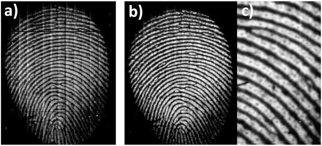
At less than 0.2 mm thick and with no bulky prisms or moving parts, the new sensors can be embedded into objects, such as mobile phones and door handles, to create invisible yet secure access control systems. Based on a 508-ppi oxide transistor backplane with a printed organic photodiode, the fabrication is compatible with flat panel display processes. The sensors read the fingerprint by detecting visible light reflected from the surface of the skin, and are able to visualize so-called level 3 details, i.e., minutia and sweat pores on top of the ridges of the finger, meeting FBI standards.
The sensors can also detect light that penetrates the skin before it is reflected. This allows them to sense a heartbeat from changes in the blood capillaries within the hand and thus verify that the print comes from a live person. Moreover, by using different photodiode materials, the sensors’ capabilities can be extended to other wavelengths, such as near infrared. This could enable new identification verification modes, such as the identification of a pattern of veins in a hand, which is believed to be even more specific to an individual than a fingerprint.
“The flexible fingerprint sensor demonstrator shows the versatility and maturity of the flexible organic photodetector technology,” says Gerwin Gelinck, CTO of Holst Centre and professor at the department of Applied Physics at the Eindhoven University of Technology in the Netherlands. “With the underlying technology already in use in the flat-panel industry, there is a fast route to manufacturing and we are working with industrial partners to take that step.”


