Microlasers hit the headlines recently after a laser 200 nm in diameter was reported by Khajavikhan et al. Such devices are opening up new possibilities to study light-matter interactions and are central to enabling new technologies such as quantum computing and integrated photonic circuits. As with most micro- and nano-technologies there are two approaches to fabricating a microlaser: bottom-up or top-down. The top-down approach is based on established semicondutor processing and generally involves a creating a microcavity using a combination of epitaxial growth, lithography, and etching, and this is the approach used to make the now famous 200 nm laser. Bottom-up fabrication involves growing the microcavity by controlled crystallisation of a nanostructure, but the size and shape of the cavity is not so controllable as with the top-down approach. Other more controllable bottom-up techniques involve encapsulating active materials in microdroplets but practical applications of these systems is hindered by other complexities, such as inherent instability of the droplets.
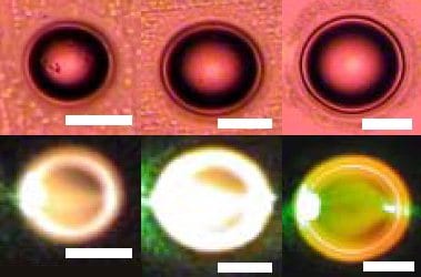
Now researchers from Nanyang Technological University have reported in Advanced Optical Materials an elegant technique for self-assembling microlasers from droplets. The cavity size is highly controllable and the lasers themselves show low losses. The team envisage using the system to probe deeper into light-matter interactions by constructing more complicated microlaser systems, such as arrays, couple cavities and cavities containing quantum dots or semiconducting nanowires.

