Printing technologies have evolved over centuries, from woodblock printing and the Gutenberg press to modern inkjet and laser printers. Current research to apply mass printing methods to materials with electronic and optical functionality could transform the manufacturing of sensors, photovoltaics, and flexible displays, among others.
In relief printing methods, ink is applied to raised images on a stamp or printing form. This stamp is brought into contact with a target substrate, such as paper, and ink is transferred from the stamp to the substrate. Controlling the transfer of ink between these surfaces is critical to print quality and reliability. Typically, the stamp is composed of a solid material, with ink only on its surface. Recently, however, scientists have discovered that a stamp with nanoscale pores interacts with the ink differently due to its high surface area and ability to store ink within the structure.
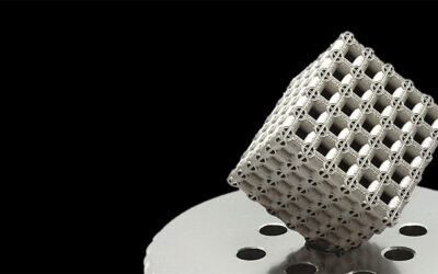
Similar to their 2D counterparts, advanced 3D printing methods offer researchers new tools to engineer materials with complex designs. One such technology, multiphoton lithography (MPL), uses a focused laser to write solid 3D objects in a liquid photosensitive resin with micron-scale precision. In this way, materials can be engineered with well-defined, microscopic pores, offering an opportunity to study and control the transfer of liquid inks using porous stamps.
To this end, our team of researchers from Sandia National Laboratories, demonstrated precise, porous stamps using MPL to engineer ink transfer in relief printing. This strategy offers deterministic control over the 3D geometry and porosity of the stamp, enabling new experiments to understand ink transfer processes in these materials.
Prior research demonstrating nanoporous stamps showed compelling prospects, which offered the opportunity to engineer the stamps directly using multiphoton lithography, to better understand what features of the microscale structure drive ink transfer.
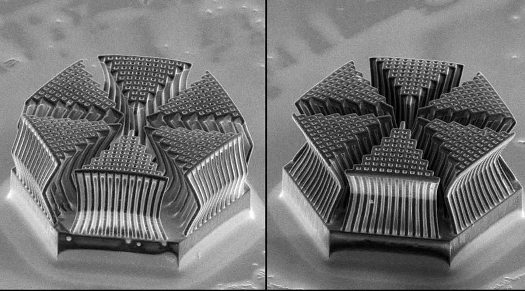
In the study, our team created porous, deformable stamps with tailored buckling behavior using a Nanoscribe MPL printer. The pores of the stamps act as reservoirs for the silver nanoparticle ink used, while also affecting capillary forces that drive interactions with the ink. The ability to design mechanical buckling into the structure could enable metered ink transfer with improved control as the stamp is deformed during the printing process.
“Once the general procedure was established, we let our imaginations run,” says lead author Michael Gallegos. “Because we could 3D print complex structures, we could test unusual designs.” One such stamp design, containing layers with different buckling characteristics and pore structures, was effective for controlling the printed film thickness. This offers a potential route to engineer stamps for greyscale patterning, in which the printed thickness is deliberately nonuniform. While this is possible for graphics by varying pixel density, it has proven challenging for continuous films needed for advanced electronic and optical applications.
By establishing the viability of MPL for stamp fabrication, our team have offered a blueprint for studies to build on this concept, both for fundamental understanding of fluid transfer and transferring this knowledge to applications at scale. We have shown that 3D printing can be used to engineer 2D printing processes, and we’re excited to see what the research community does with that design freedom.
Reference: M. A. Gallegos et. al. Investigating Porous Media for Relief Printing Using Micro‐Architected Materials, Advanced Engineering Materials (2020), DOI: 10.1002/adem.202000548

