“Perfect Extinction of Terahertz” – Adv. Opt. Mater.
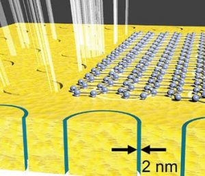
Two-dimensional materials such as graphene possess unique electrical and optical properties that are not present in bulk materials. Due to their atomic-scale thickness, however, 2D materials usually interact only weakly with electromagnetic waves, presenting challenges for realizing high-performance optoelectronic devices. Now, new research demonstrates that by confining light into ultra-small metallic gaps, it is possible to dramatically boost this interaction with graphene. As an extreme case, terahertz waves (with a wavelength of 1 mm) are squeezed into gaps about 105 times smaller, allowing them to interact with 99% efficiency with a 0.3 nm thick graphene layer.
Realization of this experiment is made possible by a new technique called atomic layer lithography to define the extremely narrow (2 nm) gaps in a metal film. While the gaps cover only 0.002% of the surface, 25% of incident THz energy passes through the metal film. The mechanism behind this dramatically enhanced transmission lies partly in the shape of the gaps themselves: as circles, they are able to efficiently funnel the THz waves along. Furthermore, since the annular gaps are so narrow, the energy density becomes very high inside the gap and near the surface. Therefore, by placing a single layer of graphene at the exit side of these gaps, 99% of the transmission is blocked since the graphene is now able to efficiently absorb the strongly confined waves. As an application of this strong absorption, the group responsible also demonstrated the construction of a high-quality THz modulator. Nanogap devices are integrated with an ionic gel gate and the enhanced intraband absorption in the graphene leads to a very large modulation depth of 80% with an operational voltage as low as 1.5 V.
In addition to graphene, such ultra-strong light-matter interactions mediated by nanogap structures could also benefit a wide range of applications involving 2D materials or biomolecules.


