Nanolithography and patterning techniques are integral to the continued development of micro and nanotechnologies. Established techniques capable of high resolution patterning of large areas remain expensive and time consuming. Researchers at the Max Planck Institute for Intelligent Systems recently combined colloidal lithography and shadow deposition techniques to present a promising flexible and precise nanolithography scheme.
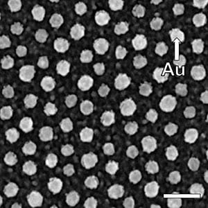
Block copolymer micelle nanolithography (BCML) is an effective large area patterning technique, but has a limited range of compatible materials. The authors combine BCML with glancing angle deposition (GLAD) to grow large area nanodot arrays and more complex nanopatterns. Combining these two techniques enables a large tunable range of particle sizes, covering the typical range of BCML (<10 nm) and nanosphere lithography (>100 nm). Simultaneous control of the particle morphology is obtained, alongside a greater flexibility in the choice of material composition.
The authors describe a three-step fabrication process to render an array of metallic nanoparticles onto the entire surface of a silicon wafer, with a total processing time of less than an hour. The resultant array is considered a multifunctional pattern, which can subsequently be used to fabricate complex secondary nanopatterns including holes, rings, domes and multilayers. An important byproduct of the secondary patterning process is the creation of colloidal solutions of hybrid nanoparticles. The nanopatterns are demonstrated in use as a large area mask for nanoimprint lithorgraphy, and as enhancers for surface enhanced Raman spectroscopy.
The combined nanolithography scheme creates smaller and more complex patterns than those achieved in independent BCML and GLAD fabrication. The demonstrated flexibility of the scheme ensures the suitability of the combined technique for use in both nanoimprint and plasmonic applications. With a ready ability to fabricate more complex nanopatterns across a range of materials, a multitude of applications for nanopatterned substrates and devices are foreseen.

