Perfect graphene is an ideal two-dimensional (2D) network of sp2–hybridized carbon atoms, and is known as the strongest material in nature. However, the practical durability of large-area polycrystalline graphene with engineering relevance has not yet been made sufficiently high to meet industrial requirements. This lack of durability is a technical impediment to development of reproducible and reliable graphene-based flexible electronic products. The strength of graphene is mainly limited by the presence of unfavorable grain structures and of defects, both of which are inevitably generated during chemical vapor deposition and transfer of graphene.
In this context, increasing the mechanical durability of large-area polycrystalline single-atom-thick materials is a necessary step toward development of practical and reliable soft electronics based on these materials. Therefore, devising an effective, easy-to-use, compatible with post processes, general strategy to improve the durability of large-area graphene is a fundamental requirement before graphene can be used in next-generation soft electronics.

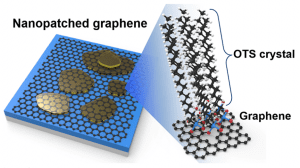
In their recent paper published in Advanced Materials, a research group from the Pohang University of Science and Technology in Korea demonstrated a new method to improve the mechanical durability of graphene films based on the introduction of chemically-attachable nanometer-thick organic patches onto a graphene surface.
The researchers showed that the surface assembly of organosilane, by weak epitaxy forms nanometer-thick organic patches on a monolayer graphene surface, can dramatically increase the material’s resistance to harsh post processing environments, thereby increasing the number of ways in which graphene can be processed. As a proof of concept, the group showed that the nano-patched graphene with the improved mechanical durability enabled stable operation when used as transparent electrode in wearable strain sensors. In addition, when applied as an electrode, it modulated the molecular orientation of deposited organic semiconductor layers and yielded favorable nominal charge injection for organic transistors.
According to their results, the use of the surface modified graphene as electrodes in organic field-effect transistors (OFETs) induced the deposited organic semiconductor layers to adopt a molecular orientation that was favorable for nominal charge injection; as a result the OFETs had superior electrical characteristics. According to the researchers “The method can increase the robustness of a wide range of 2D materials used in a wide range of applications such as electrodes and active layers in soft optoelectronic devices. These results demonstrate the potential for use of self-assembled organic nano-patches in graphene-based soft electronics. “


