Welcome to one of our guest columns, where active researchers can share their views on topics relevant to materials science. Professor Geoffrey Ozin from the University of Toronto tells us what he thinks about nanoscale silicon and its future.
One thing that has caught my eye in the last few years is the burgeoning activity and potential technological impact of research on new kinds of nano silicon, made from one of the most abundant and green materials on earth.
And I am not talking about the utilization of top-down nano silicon for integration as electrical components in the incredible shrinking world of m(o)ore powerful and faster microelectronics.
I am rather referring to the notable intensification of research on bottom-up myriad forms of nano silicon for everything other than microelectronics!
Nano silicon materials and structures fashioned into almost every conceivable size and shape, chemically functionalized surface and overall form, is beginning to play a prominent role in the bottom-up assembly and top-down fabrication of a cornucopia of nano stuff exemplified by chemical and biological sensors, fluidic field-effect transistors and flow monitors, printed ink backplane thin-film transistors, computer memories, radio-frequency identification tags, proton-conducting membranes for hydrogen–oxygen fuel cells, high-capacity lithium ion battery anodes, photocatalysts, solar cells, solid-state lighting, optical interconnects, ultrahigh frequency oscillators, photonic crystal optical cavities and waveguides, electronic eyes, bioinspired self-cleaning anti-reflection coatings, nutrients in functional foods and beverages to enhance bone health, biodegradable luminescent porous drug delivery systems, and biocompatible implantable medical devices. This overly long list just names a few prominent reports for nano silicon that one can easily search in the 2007-2010 scientific literature.
Curiously nano silicon has even been invoked to explain the origin of the observed extended red emission (ERE) from interstellar dust. And the purported non-toxicity and biocompatibility of nano silicon allows it to be marketed as a “Green” material in the emerging field of medical theranostics!
As a self-confessed proponent of nanochemistry I note that many of these new applications for nano silicon are enabled by bottom-up synthetic strategies. These are providing increasingly impressive command over the size and shape, dopants and defects, surface structure and surface functionalization of nano silicon and the self-assembly of these nano silicon forms into purposeful constructs. And the ultimate success of most of these applications will depend on the scalability and processibility, cost effectiveness and manufacturability of nano silicon in these varied forms.
It is a truism that chemistry is the beginning of the nanomaterials food chain and we are now seeing this in creative synthetic routes for preparing silicon in a range of forms beyond those documented for the usual nanocrystals, nanorods and nanowires. These syntheses include gas, solution, liquid and solid phase chemical, photochemical, thermochemical and electrochemical pathways to nano silicon with self-assembled architectures often directed by templates and lithographic patterns.
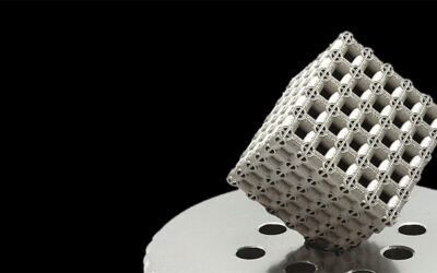
Using these methods one can gain access to all-silicon-based amorphous nanoscale colloids, zig-zag, buckled and porous nanowires, straight and buckled nanoribbons, nanotubes, nanosheets, nanospheres, nanoshells, nanocrystal nanospheres and periodic mesoporous materials. And at slightly larger yet submicron length scale we find a treasure trove of silicon-based macroporous crystals (like the one shown in the figure above), meshes and membranes, 2D- and 3D-folded thin-film shapes, and even replicated biomineral and geomineral shapes like diatom microskeletons and opals.
Of course evoking light from indirect bandgap silicon has always been and continues to be a challenge for light-emitting diodes and lasers. And then along came brightly emissive porous silicon in the late eighties and the rest is history. For the new nano silicon forms to display bright tuneable wavelength photoluminescence arising from quantum and spatial confinement effects, at least one dimension of the nanostructure has to be below the dimensions of the 5 nm exciton in silicon. In this context, it has been recently shown that the color of nano silicon can be tuned across the visible spectrum in an entirely different way involving the strong resonant scattering of white light from silicon nanowires with different diameters. And as expected, the main challenges for successfully handling, processing and exploiting the unique properties of nano silicon in this tiny size regime are long term control of its surface oxidation and its colloidal stability. The electrically pumped silicon laser is a still a holy grail!
One can appreciate from the above that while the reign of the Silicon Samurai is still the top-down computer chip, there is a flood of opportunities for fundamental research on bottom-up forms of nano silicon that could give birth to the Nano Silicon Samurai spawning exciting new nanotechnologies potentially able to change the world as we all experienced with the silicon transistor.
Image Credit: Nicolas Tetreault
Do you think the Nano Silicon Samurai will soon reign? Let us know in the comments below!


