 Welcome to one of our guest columns, where active researchers can share their views on topics relevant to materials science. Professor Geoffrey Ozin from the University of Toronto talks about where we are in solar cell research today.
It seems like the whole world is working on solar cells; trying to make them better, cheaper and safer to cope with the looming global energy drought.
Solar cells today come in three main flavours: Generation I – high efficiency, high cost; Generation II – low efficiency, low cost and Generation III – high efficiency, low cost. Most of the market activity seems to be concentrated around Generation I and II while Generation III remains mainly in the laboratory research phase awaiting a big breakthrough.
Crystalline silicon, expensive to produce but exhibiting high efficiency, stands aloof and alone in Generation I, with its performance capped by the thermodynamic Schockley–Quiesser 33% limit, defined by electronic bandgap and hot electron losses. Despite its high cost, crystalline silicon makes up the vast majority of cells being employed in real-world applications today.
Vying for market dominance and accepting lower efficiency in exchange for lower cost are Generation II thin film solar cells utilizing semiconductor materials such as amorphous silicon, cadmium telluride, copper indium gallium selenide, nanocrystalline titania, organic molecules and polymers.
Generation III solar cells are attracting a lot of research activity these days and can be considered to synergistically integrate electrical, optical and photonic (nano)materials chemistry, materials science and engineering approaches to create low-cost and high-efficiency solar cells designed to beat the Shockley-Quiesser limit. Despite all of the attention Generation III solar cells have received, they are still a very long way from achieving their target efficiencies.
Different solar cell architectures and strategies currently being explored to achieve Generation III cost and efficiency goals include multi-junction tandem, multi-exciton, up-and down-conversion, texturing, intermediate band states, intermediate reflectors, photonic crystals, and plasmonic and optical concentrators.
Generation III is proving to be a (nano)materials playground for creative bottom-up chemistry ways to simultaneously enhance solar cell performance while keeping the cost down.
One thing I have noticed in recent Generation III solar cell research is the increasing use of self-assembled monolayer or multilayer films of nanospheres with diameters from nanometers to microns. These nanospheres may serve a number of purposes, for example as templates for texturing semiconductor surfaces using the patterning technique of nanosphere lithography. Texturing causes multiple scattering of light and so increases the optical path length of light inside the active semiconductor material, thus increasing its absorption while using a smaller thickness of material, saving on cost.
Sphere films are also being employed to enhance the harvesting of light and boost the generation of electron hole pairs using different kinds of optical and photonic effects.
Noteworthy in this respect is the use of optically transparent and electrically conductive zinc oxide inverse colloidal crystal film as an intermediate reflector in a silicon tandem solar cell to enhance its performance, using the cell architecture illustrated in the figure (Reproduced with permission from Opt. Exp., 2010, 18, 4478). The role of the intermediate reflector layer between the a-Si:H (Eg = 1.7 eV) and µc-Si:H (Eg = 1.1 eV) junctions shown in the figure is to return incident photons of energy greater than 1.7 eV to the upper a-Si:H cell, where they have a second chance to be absorbed and where more of their energy will be available than would be to the 1.1 eV layer due to thermalization losses. To optimize the operation of this tandem solar cell the goal is to obtain the same current in the top and bottom components of cell. The aforementioned intermediate reflector is designed to boost the current generated in the upper cell while transmitting photons of lesser energy to the underlying µc-Si:H cell.
Another approach to boost performance involves the placement of spheres with encapsulated plasmonic nanoparticles on an electrode of a dye-sensitized solar cell, whereby trapping of light occurs through a combination of multiple light scattering and local electromagnetic field enhancement that serve to amplify the absorption of light by the dye and enhance the photogeneration of electrons and holes.
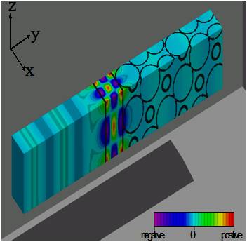
A colloidal crystal film made of silica spheres has also been utilized as a back reflector optically coupled to a silicon or nanocrystalline titania thin film in a silicon or dye-sensitized solar cell. The idea of this cell architecture, illustrated in the figure for the case of a thin silicon film (centre) sandwiched between a silica colloidal crystal film (right) and a glass substrate (left), is to enhance the effective optical path length of light in the active semiconductor. This occurs through a combination of transverse reflected and longitudinal diffracted modes, which serve to enhance the localization of light and its absorption in the semiconductor and hence the efficiency of generating electron hole pairs, manifest as an amplification in the photoconductivity compared to the case where a silver mirror or air replaces the silica colloidal crystal film. (Figure reproduced with permission from Adv. Mater. 2008, 20, 1577).
Colloidal crystals assembled from nanospheres have also been used in solar cells for their ability to control light be slowing it, as well as simply reflecting it. Silicon inverse colloidal crystals can be synthesized in both intrinsic and extrinsic n-doped and p-doped forms. The intrinsic inverse silicon colloidal crystal has been used as i-layer, in a p-i-n amorphous silicon solar cell, to exploit slow light amplification of the absorption of incident light in i-layer in an attempt to improve cell performance.
Nanospheres have also been used for their ability to individually confine light: whispering gallery modes associated with spheres in a monolayer sphere film located on the electrode of a dye-sensitized solar cell have been used to enhance the coupling of incident light to the absorbing dye in an effort to improve the performance of the solar cell.
While there is still much research to be done to understand how to improve the efficiency of Generation III architectures it seems to me from all this recent activity that nanospheres and solar cells are on a roll!

