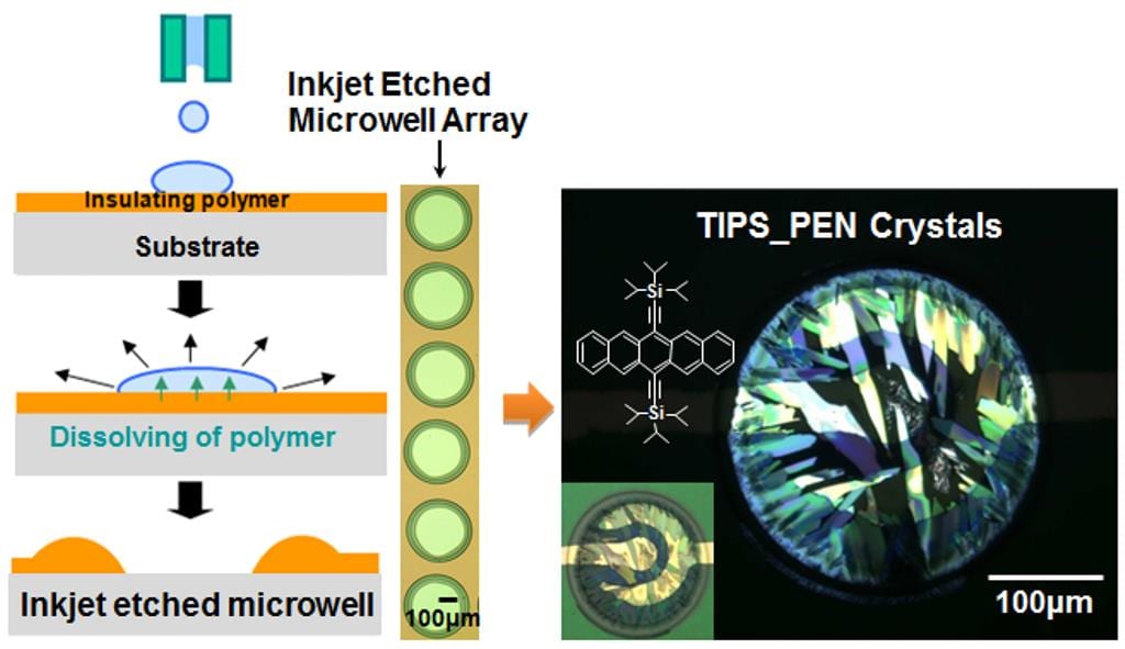
High-precision printing of organic semiconductors—essential for plastic electronic applications—demands new techniques that work for large-area and flexible substrates, and above all else, are cost-effective and have high throughput. A new approach based on inkjet printing reported by the group of Kilwon Cho (Pohang University of Sciences and Technology, Korea) satisfies these criteria and opens a range of new possibilities in the area of organic electronics.
The beauty of this method lies in its simplicity. Briefly, droplets of solvent have previously been used to etch a thin polymer film to create microwells. These wells, which expose the underlying functional layers, can provide connectivity in organic transitors. Now, using inkjet-printing, Cho and co-workers have created regular arrays of microwells (formed via the coffee-ring effect as the polymer film is dissolved by the injet-printed solvent droplets) and used these to confine semiconductors droplets.
The crystalline structure of the semiconductor is critical in achieving the desired electrical properties and performance in organic field-effect transistors. Two different polymers were used to form microwells with either hydrophilic or hydrophobic walls. Confined within hydrophilic walls on a hydrophobic surface, the molecular orientation in the crystals was found to be highly ordered. This corresponded to good electrical performance, proving that this method is well suited for the fabrication of large-scale flexible organic transistors.

