A strategy for placing bezel-less image sensors for electronic devices over the entire surface of a tetrahedral, 3D sensor is demonstrated.
![Transforming Planar Electronic Devices into 3D Structures [Video]](https://www.advancedsciencenews.com/wp-content/uploads/2018/07/adma201801256_ASN-image_smaller.png)
A strategy for placing bezel-less image sensors for electronic devices over the entire surface of a tetrahedral, 3D sensor is demonstrated.
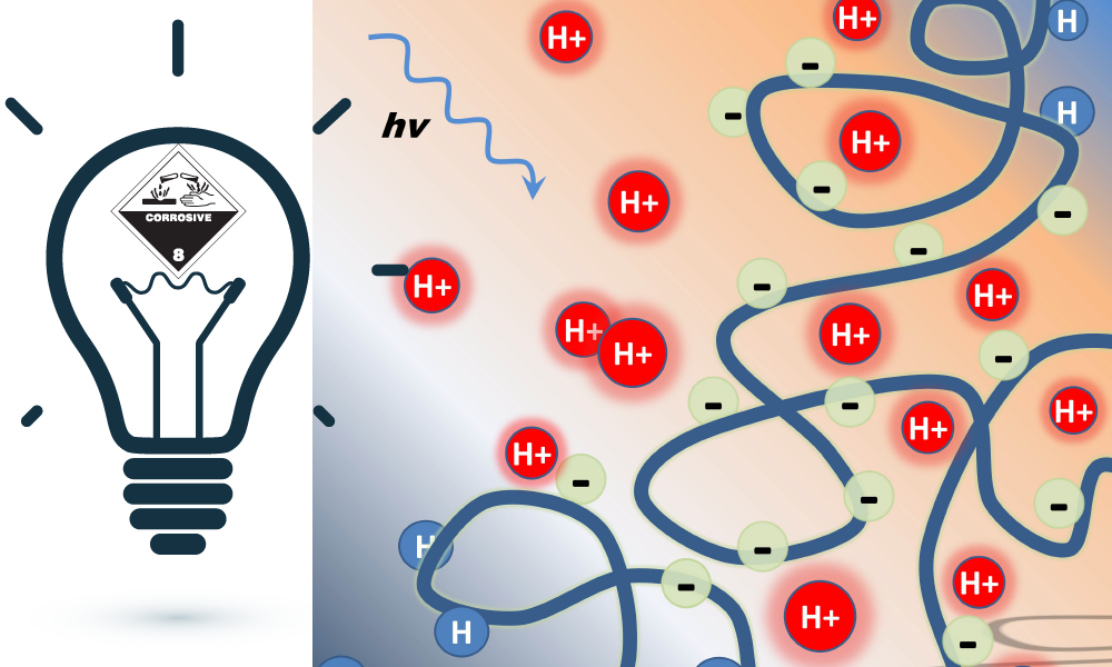
Polymeric Photoacids allow the localized production of protons while the polymerization is straight forward and avoids the use of protecting groups and extra steps in the synthesis.
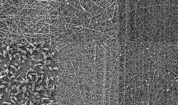
A team of scientists from Belgium investigated the plasma‐induced chemistry in organic solutions of polylactic acid (PLA), and their effects on the resultant PLA nanofibers.
The broad applications of LOV domains in optogenetics are reviewed.

Disposable and flexible electronics made from paper could provide a cost-effective alternate to current electronic device materials.
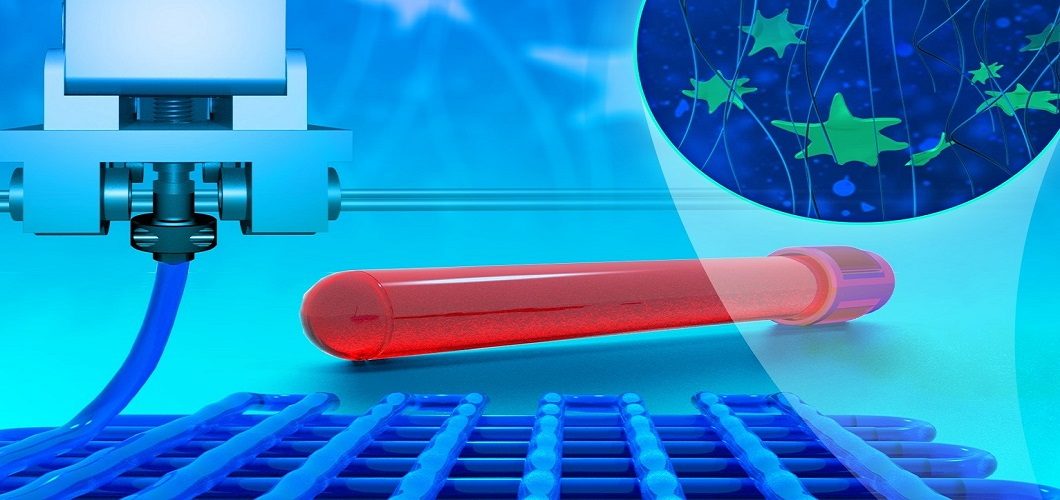
![Unravelling the Cytokine Secretion Process of Single Cells with a Novel Biosensor [Video]](https://www.advancedsciencenews.com/wp-content/uploads/2018/07/smll201800698_ASN_image_3.jpg)
A nanobiosensor is developed that performs real-time analysis of single-cell cytokine secretion, enabling the development of new therapies for diseases.
Check out the latest covers of Advanced Healthcare Materials!
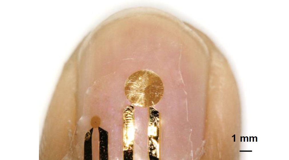
A wearable fingernail sensor that can collect thermal data of the nailbed tissue in real-time is developed.

Exceptionally stable and colourful light-emitting nanofibers are synthesized in a simple one-pot process.

Phosphors are less excited by electrons than by their antiparticles.
 New theory suggests gravity is not a fundamental force
 Quantum entanglement visualized for the first time ever
 Scientists take a closer look at rare particles called hypernuclei
 French WEST reactor breaks record in nuclear fusion
 Higgs boson may be driving the Universe’s expansion
 Researchers take a glimpse at the structure of rare tetraquarks
 Black hole images deliver a deathblow to alternative theory of gravity
 An anti-inflammatory peptide may hold the key to low-back pain relief
 CERN scientists search for new physics in unusual energy patterns linked to hidden particles
 String theory provides a new take on the expansion of the Universe