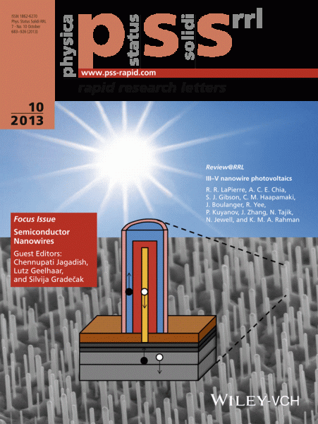
Over the past decade, research on semiconductor nanowires has become one of the most active fields in nanoscience and technology, and work in this area continues to expand. One particularly exciting aspect of this research field is its interdisciplinary nature that brings together scientists trained in physics, chemistry, materials science, electrical engineering, biology, and medicine. The purpose of a new Focus Issue in pss (Rapid Research Letters) guest-edited by Chennupati Jagadish (ANU, Canberra and pss Editorial Advisory Board member), Lutz Geelhaar (Paul-Drude-Institut Berlin) and Silvija Gradecak (MIT, Cambridge) is to provide a status overview in the form of Reviews@RRL as well as a snapshot of ongoing activities.
Semiconductor nanowires are structures that are characterized by their high aspect ratio and a diameter that typically does not exceed 100 nm. The nanoscale size and the quasi one-dimensional shape offer unique opportunities to control properties of semiconductors such as density of states, transport of electrons, and interaction with photons. Thus, these objects are considered as building blocks for the next generation of electronics, photonics, energy, sensing, and biomedical applications.
Another important feature of nanowires is the possibility to grow heterostructures of materials with large lattice and thermal mismatch without creating dislocations. This advantage over planar films provides an unprecedented flexibility to create a broad range of structures with a combination of different materials that may lead to the observation of exciting physical phenomena or novel functionalities for applications. In particular, nanowires may pave the way for the integration of microelectronic devices on silicon with optoelectronic and photonic devices based on compound semiconductors.
Both the ten Review@RRL articles listed below and further 21 Rapid Research Letters in this Focus Issue cover a wide scope of topics, methods, and materials ranging from growth and theoretical approaches to thermoelectric, electronic, optoelectronic and photovoltaic properties, applications and devices. Essentially the entire range of inorganic semiconducting materials is covered in this Focus Issue, from silicon and germanium, both narrow and wide bandgap II–VI, III–V, and IV–VI compound semiconductors to semiconducting oxides.
Reviews@RRL in the Focus Issue on Semiconductor Nanowires
Highlight: III–V nanowire photovoltaics: Review of design for high efficiency [Free access]
R. R. LaPierre, A. C. E. Chia, S. J. Gibson, C. M. Haapamaki, J. Boulanger, R. Yee, P. Kuyanov, J. Zhang, N. Tajik, N. Jewell and K. M. A. Rahman
Advances in semiconductor nanowire growth on graphene [Open Access]
A. Mazid Munshi and Helge Weman
First principles studies of structural, electrical and magnetic properties of semiconductor nanowires
Marta Galicka, Ryszard Buczko, Perla Kacman, Erika N. Lima, Tome M. Schmidt and Hadas Shtrikman
Thermal conductivity of silicon nanowires: From fundamentals to phononic engineering
Gang Zhang and Yong-Wei Zhang
Thermoelectricity in semiconductor nanowires
Jungwon Kim, Je-Hyeong Bahk, Junphil Hwang, Hoon Kim, Hwanjoo Park and Woochul Kim
Nanofunctional gallium oxide (Ga2O3) nanowires/nanostructures and their applications in nanodevices
Sudheer Kumar and R. Singh
Silicon nanowires – a versatile technology platform
Thomas Mikolajick, André Heinzig, Jens Trommer, Sebastian Pregl, Matthias Grube, Gianaurelio Cuniberti and Walter M. Weber
Group III nitride core–shell nano- and microrods for optoelectronic applications
Martin Mandl, Xue Wang, Tilman Schimpke, Christopher Kölper, Michael Binder, Johannes Ledig, Andreas Waag, Xiang Kong, Achim Trampert, Frank Bertram, Jürgen Christen, Francesca Barbagini, Enrique Calleja and Martin Strassburg

