Welcome to the latest selection of recent top articles in the physica status solidi journals. Get a glimpse of our publication spectrum and visit our pages by clicking on any of the DOI links below.
High reliability amorphous oxide semiconductor thin-film transistors gated by buried thick aluminum [Rapid Research Letter]
Dongxiang Luo, Linfeng Lan, Miao Xu, Hua Xu, Min Li, Jianhua Zou, Hong Tao, Lei Wang, and Junbiao Peng
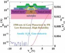 In this Letter, an indium-zinc-oxide thin-film transistor (IZO-TFT) with a 1500 nm thick aluminium gate is demonstrated. The Al gate assembly was planarized by a photoresist, and then was further anodized to form a layer of Al2O3 as gate dielectric. The thick Al has low-hillock density and low resistance. This IZO-TFT shows high mobility, high reliability and good electrical stability.
Phys. Status Solidi RRL (2012) DOI 10.1002/pssr.201206303
Copper-alloyed ZnS as a p-type transparent conducting material [Advanced Materials Physics]
A. M. Diamond, L. Corbellini, K. R. Balasubramaniam, S. Chen, S. Wang, T. S. Matthews, L.-W. Wang, R. Ramesh, and J. W. Ager
 A p-type wurtzite transparent conducting material (TCM) was synthesized from earth abundant elements. The potential application of this TCM was demonstrated through its use in a rectifying transparent diode. By utilizing a wurtzite transparent p-type conductor, photovoltaic cells could potentially be manufactured using new types of materials. In addition, the development and optimization of such a p-type TCM could open new frontiers in the development of transparent transistors, light emitting diodes, electro-chromic windows and a wide range of additional optoelectronic devices.
Phys. Status Solidi A (2012) DOI 10.1002/pssa.201228181
Device efficiency of organic light-emitting diodes: Progress by improved light outcoupling [Review Article]
Wolfgang Brütting, Jörg Frischeisen, Tobias D. Schmidt, Bert J. Scholz, and Christian Mayr
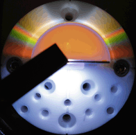 Organic light-emitting diodes (OLEDs) are efficient large-area light sources facing their market entry. Still, the enhancement of light outcoupling from the multi-layer thin film structures remains a major challenge. This review introduces the working principles of OLEDs and gives an overview of ongoing efforts to improve their efficiency, in particular by extracting more light. As an example, the photograph shows a white OLED where light emission from trapped modes is enabled by a high-index prism.
Phys. Status Solidi A (2012) DOI 10.1002/pssa.201228320
In(Ga)As/GaAs site-controlled quantum dots with tailored morphology and high optical quality [Feature Article]
C. Schneider, A. Huggenberger, M. Gschrey, P. Gold, S. Rodt, A. Forchel, S. Reitzenstein, S. Höfling, and M. Kamp
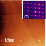 One of the most important challenges in seeking for scalable approaches for quantum information architectures based on optically active single quantum dots (QDs) in semiconductors is gaining control over the emitter’s position. One concept to achieve well-ordered arrays of In(Ga)As quantum dots fabricated on the most commonly used (001) oriented GaAs substrate is based on principles of directed nucleation on nanoholes, and it is approaching now a high level of maturity. In this Feature Article, the authors discuss and review growth and fabrication strategies allowing for the realization of perfectly ordered In(Ga)As QD arrays, comprising optical properties comparable to their self-assembled counterparts.
Phys. Status Solidi A (2012) DOI 10.1002/pssa.201228373
Embedded metal nanopatterns for near-field scattering-enhanced optical absorption [Advanced Materials Physics]
Fan Ye, Michael J. Burns, and Michael J. Naughton
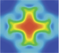 Optimizing light trapping in thin-film solar cells has been intensively investigated in recent years. Ye, Burns and Naughton use simulations to show that subwavelength-dimensioned metal nanopatterns embedded in a thin film of amorphous silicon (a-Si) significantly enhance its optical absorbance, with more than 300% increase at 800 nm wavelength. Embedding such metal patterns inside a photovoltaic absorber concentrates the electromagnetic field associated with enhanced near-field scattering in the vicinity of the pattern. Configured with an insulating coating, this optical metamedium is proposed as a means to increase the efficiency of thin film solar cells.
Phys. Status Solidi A (2012) DOI 10.1002/pssa.201228459
Enhanced light-extraction from a GaN waveguide using micro-pillar TiO2–SiO2 graded-refractive-index layers
F. W. Mont, A. J. Fischer, A. N. Noemaun, D. J. Poxson, J. Cho, E. F. Schubert, M. H. Crawford, D. D. Koleske, and K. W. Fullmer
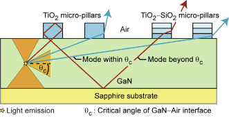 In GaInN light-emitting diodes (LEDs), the high-refractive-index contrast at the semiconductor–air boundary produces total internal reflection and guided modes within the LED chips thereby significantly limiting their light-extraction efficiency (LEE). To analyze the extraction of light, Mont et al. have designed and fabricated a GaN waveguide LED test structure with micro-pillar arrays. Electroluminescence measurements of waveguide LEDs with pillar diameters in the 2–10 μm range reveal increasing LEE with decreasing pillar diameter. A 54% enhancement is demonstrated for GaN waveguides cladded with a triangular lattice of graded-index (GRIN) TiO2–SiO2 micro-pillars of 2 μm diameters compared to waveguides with unpatterned GRIN layer.
Phys. Status Solidi A (2012) DOI 10.1002/pssa.201228295
Molecular chirality at surfaces [Review Article]
Karl-Heinz Ernst
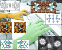 Chirality deals with the handedness of things. It has consequences in many disciplines, including nuclear physics, pharmacology, fragrance chemistry and molecular biology. When molecules adsorb at surfaces, mirror symmetry breaking is a common phenomenon and installs therefore handedness to the adsorbate. This Review Article is a digest of principles of mirror symmetry breaking upon adsorption and gives a topical review of molecular chirality at surfaces. Many different aspects of adsorption and self-assembly of chiral and prochiral molecules in two-dimensional systems at surfaces are discussed.
Phys. Status Solidi B (2012) DOI 10.1002/pssb.201248188
Phase Change Materials: Chalcogenides with remarkable properties due to an unconventional bonding mechanism [Feature Article]
Matthias Wuttig
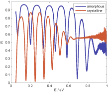 Phase Change Materials are characterized by a unique property combination which encompasses a pronounced property contrast between the amorphous and crystalline state, as well as rapid crystallization. This property portfolio is ideally suited for data storage applications. In his Feature Article, Matthias Wuttig reviews the understanding of the relationship between the properties of phase change materials and their mechanism of chemical bonding, in an attempt to provide a generic explanation for many of the unconventional properties of phase change materials.
This Feature Article will be published in a Special Issue on “Phase-change memory: Science and applications”, dedicated to Stanford R. Ovshinsky on the occasion of his 90th birthday.
Phys. Status Solidi B 249, 1843 (2012) DOI 10.1002/pssb.201200582
Capturing the re-entrant behaviour of one-dimensional Bose–Hubbard model
M. Pino, J. Prior, and S. R. Clark
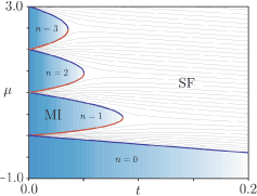 The Bose–Hubbard model (BHM) is an archetypal quantum lattice system exhibiting a quantum phase transition between its superfluid (SF) and Mott-insulator (MI) phase. Unlike in higher dimensions the phase diagram of the BHM in one dimension possesses regions in which increasing the hopping amplitude can result in a transition from MI to SF and then back to a MI. This type of re-entrance is well known in classical systems like liquid crystals yet its origin in quantum systems is still not well under-stood. Pino et al. study in detail the predictions of three different and widely used approximations: a multi-site meanfield decoupling, a finite-sized cluster calculation, and a real-space renormalization group (RG) approach. It is shown for the first time that RG does capture the re-entrant feature and constitutes one of the simplest approximation able to do so.
Phys. Status Solidi B (2012) DOI 10.1002/pssb.201248308
Stability of 71° stripe domains in epitaxial BiFeO3 films upon repeated electrical switching
Florian Johann, Alessio Morelli, and Ionela Vrejoiu
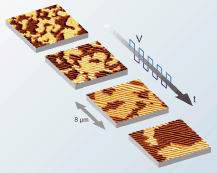 The 71° stripe domain patterns of epitaxial BiFeO3 thin films are frequently being explored to achieve new functional properties, dissimilar from the BiFeO3 bulk properties. We show that in-plane switching and out-of-plane switching of these domains behave very differently. In the in-plane configuration the domains are very stable, whereas in the out-of-plane configuration the domains change their size and patterns, depending on the applied switching voltage frequency.
Phys. Status Solidi B (2012) DOI 10.1002/pssb.201248329


