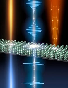
A new territory for metamaterials. Metamaterials are man-made structures exhibiting advantageous electromagnetic properties that are not naturally available. Optical metamaterials consist of arrays of submicron size units that act as “man-made atoms” interacting with electromagnetic waves in unconventional ways and allowing one to “tune” (or customize) the electromagnetic properties of a designed material. Metamaterials have demonstrated novel properties, such as negative refraction (where light rays are refracted at a different angle than normally expected), invisibility cloaking, and super-resolution imaging.
 Dielectric metamaterials use high refractive-index materials to significantly reduce optical energy losses that are normally associated with conventional metamaterials made from metals. Most dielectric metamaterials at optical frequencies are made from silicon and have already shown effective applications in nonlinear optical conversion, spectral filtering, and advanced wave-front engineering. However, using silicon remains a challenge for achieving efficient light emission, strong second-order nonlinear optical effects or 3D metamaterials.
Sheng Liu, Igal Brener, Mike Sinclair and other co-workers from Sandia National Laboratories overcame these limitations by demonstrating both two-dimensional and multilayer (3D) dielectric metamaterials made from III-V semiconductors (elements from groups III and V on the periodic table) using a monolithic fabrication process. These metamaterials did not contain silicon, and the fabrication method avoided using complex flip-chip bonding processes, which are conventionally used to create high refractive-index contrast in other metamaterial approaches. Instead, the necessary high refractive-index contrast was achieved by selectively oxidizing semiconductors to their native oxides. The wavelengths of the electromagnetic resonances could also be tuned by varying the nanodisk diameters on the dielectric metamaterials.
This technique simplifies dielectric metamaterial fabrication and enables more complicated architectures (such as 3D metamaterial structures) to provide new degrees of freedom in device engineering. For example, this work can be used to construct multilayer (3D) III-V semiconductor dielectric resonator arrays, whose reflectivity exceeds that of a gold mirror over a broad spectral range. The ultrathin (less than 2 μm) multilayer metasurfaces could also recompress femtosecond optical pulses (1013 times shorter than a second) that were broadened after passing through some length of dispersive glass. The recompression of these pulses is useful for applications such as multiphoton microscopy and lithography. This fabrication method could be used to construct extremely compact optical components, significantly lowering manufacturing costs, sizes, and energy consumption. Extension of this dielectric metamaterial fabrications strategy could also lead to fully 3D, low-loss metamaterials, at optical frequencies which is a long-standing challenge for metamaterial fabrication. Finally, the III-V semiconductor metamaterials can lead to novel active applications such as efficient nonlinear frequency converters, light emitters, detectors, and modulators.


