The development of photovoltaics and novel solar cell materials is currently the focus of intense research due to increasing energy demand, the effects of the climate change, and the shortage of the non-renewable energy resources.
Among newly explored materials indium sulfide (In2S3) has been posed as a promising candidate for the replacement of CdS buffer layers in solar cell devices due to its transparency, tunability of physical properties and its lower toxicity. Similarly, hexaindium heptasulfide (In6S7) presents interesting properties as (light) absorber material, making the In-S system of interest for the field of photovoltaics.
In addition to the combination of intrinsic properties of the materials used in the fabrication of solar cells, the way they are configured, i.e. their morphology and structuring, plays a fundamental role optimizing the cell efficiency. Micro and nanostructuring the window and/or the absorber layers is usually adopted as a strategy to reduce the reflection losses as well as to increase the collection of the photogenerated carriers.
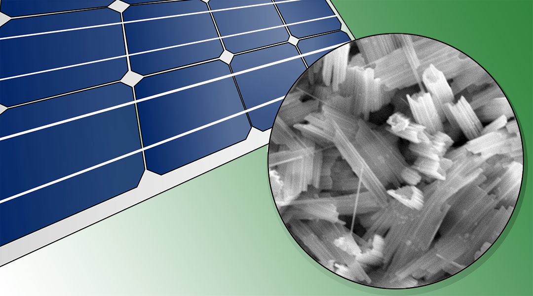
In their paper, researchers from the Complutense University of Madrid in Spain report the fabrication of In2S3 microcolumns as well as novel In6S7 nanowires with controlled phase and morphology. The structures were grown following a thermal evaporation-deposition method where both the evaporation and deposition temperatures can be adjusted separately to tune the obtained final products.
The researchers observed that In6S7 tend to form a thin layer over most of the obtained In2S3 structures. The combination of In2S3, with a larger and tunable bandgap, and In6S7 with a bandgap below 1 eV could permit the eventual realization of microstructured all In-S based heterojunction solar cells with simplified design and enhanced absorption, where In2S3 may act as window and high bandgap absorber, leaving In6S7 as the low bandgap absorber.
There is however an important issue which should be addressed before such structures could be used in solar cell technology, as the method employed by the researchers leads to heavily n-type degenerated In6S7 nanowires, which is usually detrimental for the performance of the cells. Nevertheless, the origin of this intrinsic degeneracy is attributed to S vacancies and other possible defects, which could leave room for further improvement.


