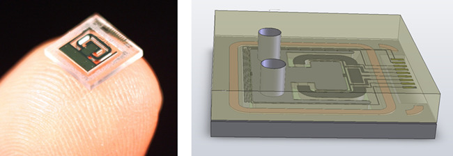
Contemporary developments in digitalization and the internet of things create a high demand for a multitude of sensors. Besides outstanding measurement performance, many applications require miniaturization of the sensor, together with ubiquitous attributes like low price and high reliability. All of these can be achieved by utilizing Microsystems Technologies, which make use of crystalline silicon as the base material.
Over the last several decades, microelectronics have been continuously miniaturized, with higher reliability and functionalities due to the high accuracy of the silicon and the use of lithographic methods. The high reproducibility of this technology and the integration of many devices on a single wafer have enabled superior properties. Additionally, for advanced sensors and actuators, mechanical functionalities have been introduced to the devices, commonly known as micro electromechanical systems (MEMS).

The first MEMS developments were pressure sensors and the silicon print head of the HP inkjet printers in the 1980s, followed by the fully integrated single‐chip accelerometer in 1993 by Analog Devices and a micro‐machined silicon tuning‐fork gyroscope by Draper Labs in 1993.
More recent developments involve the use of plasma as an etching technique for silicon. Besides deposition of thin films by plasma techniques, like sputtering or plasma enhanced chemical vapor deposition (PECVD), etching processes, such as highly anisotropic etching of silicon by deep reactive ion etching (DRIE), have enabled production of surface micromachined MEMS, which have become a huge commercial success story.
For more information of the use and success of plasma for microfabrication read the latest special issue on Plasmas for Microfabrication of Plasma Processes and Polymers.


