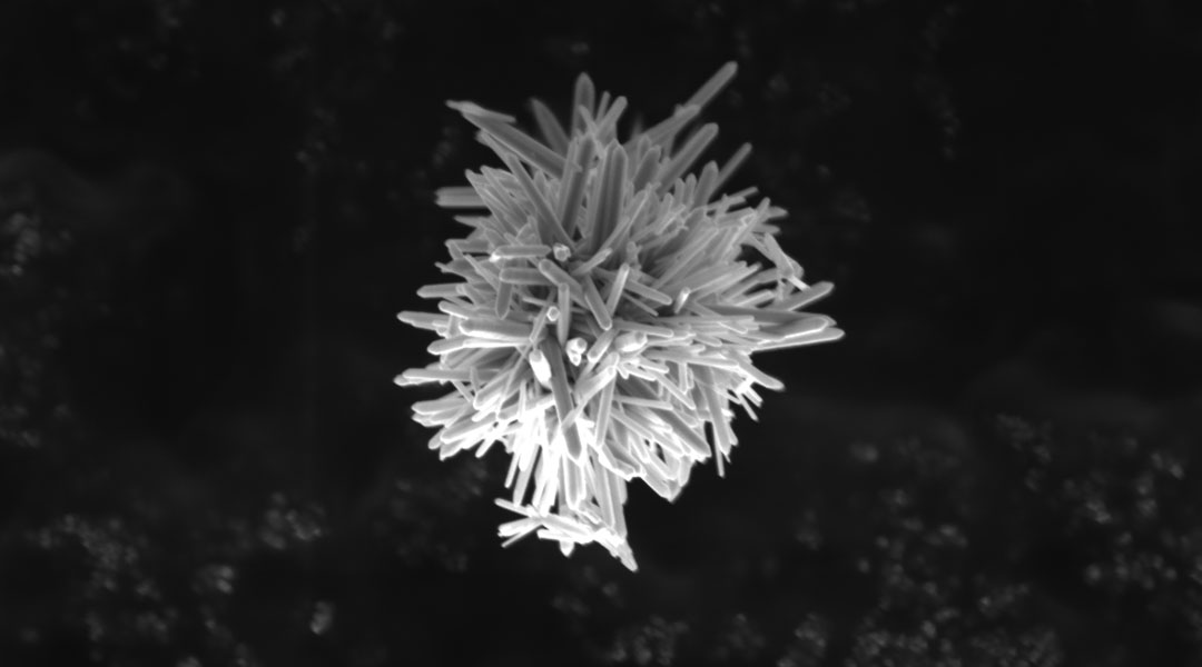
Biofilm-killing micromotors. Image credit: Martin Pumera et al.
Art is born of the observation and investigation of nature — Marcus Tullius Cicero. In this edition of “This month in pictures“, we gathered beautiful image published in our journals, which help us better connect with the creative, or perhaps even human, side of science. These pictures offer snapshots of months or even years of labor, capturing groundbreaking technologies and innovations that will hopefully one day change the world for the better.
Building blocks of synthetic biology
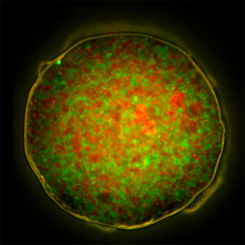
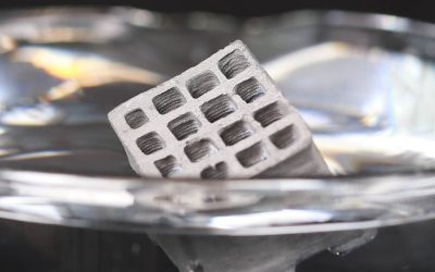
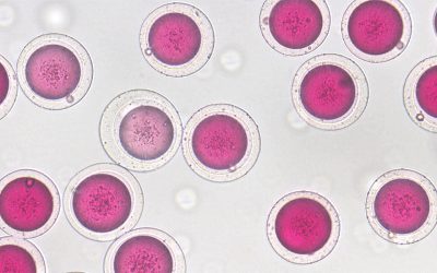
Recreating the structure of living tissue is one of the major hurdles in the field of synthetic biology and biological engineering. One way to overcome this is by relying on protocells as foundational units to build free-standing structures with complex architecture. University of Bristol-based Pierangelo Gobbo and colleagues are doing just that. The team has found a way to create water-stable protocells using a mold, which can then be used to build tissue of any shape or size (as shown here). Their work was published this month in Advanced Materials.
Patterning on the nanoscale
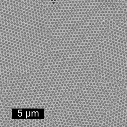
This SEM image of a Au–Au nanoring array demonstrates the capabilities of a new patterning technique developed by John de Mello, Sihai Luo, and their team. Through molecular self-assembly and physical peeling, they were able to control the gap-width of metallic nanogaps — fundamental components of nanoscale photonic and electronic devices — from 30nm down to just 3nm. This work, published in Advanced Materials, extends the range of metallic nanostructures that can be fabricated over large areas, with the hope that it will find application in molecular electronics, plasmonics, and biosensing.
Controlling robots with liquid crystals
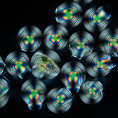
How can liquid crystals help robots understand their environment better? In a new study published in Advanced Functional Materials, Yong Geng and colleagues demonstrate how liquid crystals molded into spheres can reflect a narrow set of wavelengths to communicate with machines. In using these retroreflectors with ultraviolet and infrared wavelengths, their footprint is invisible to the human eye. Given this, the researchers suggest that these reflectors can be used to help autonomous robots navigate densely populated environments, such as cities, without the reflectors being aesthetically distracting.
Genes for happiness
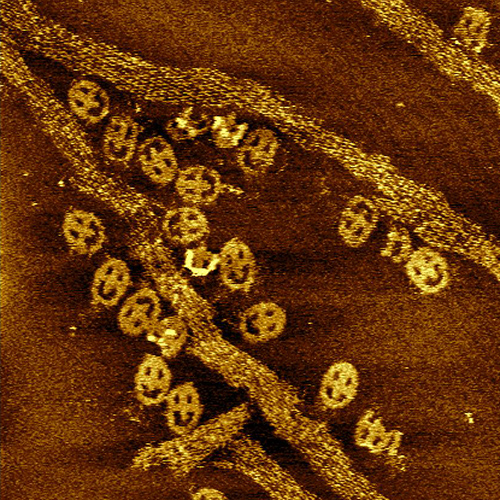
Smile, you’re on camera! Well, actually, an atomic force microscopy image. This fun and happy rendering is the work of Jonathan Burns at University College London, publishing in Small, who has functionalized DNA fibers (visible here) with self-made DNA-origami smileys. The interaction of specific DNA base pairs with one another makes DNA an ideal material for folding into structures on the nanoscale (these smileys are less than 100nm in size). Originally a mere novelty, this construction method has exploded in recent years and promises potential in materials, physical, and biological sciences.
Building better bone
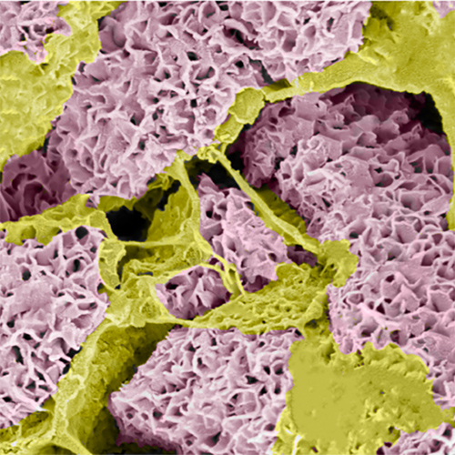
In a surgical context, bone defects are often treated with bone grafts. However, this practice is limited by the availability of donor tissue and the risk of graft rejection. Building new tissue with a patient’s own cells would help to address these problems. This scanning electron microscope image shows the formation of hydroxyapatite microstructures (in purple) in a scaffold that consists of an inorganic material and cells that are specialized for assisting bone formation. The shape of these bone scaffolds, reported by Ruei-Zeng Lin, Juan Melero-Martin, and their co-workers in Advanced Healthcare Materials, can be tailored to meet the requirements of specific bone defects.
Self-propelled micromotors destroy bacterial biofilms
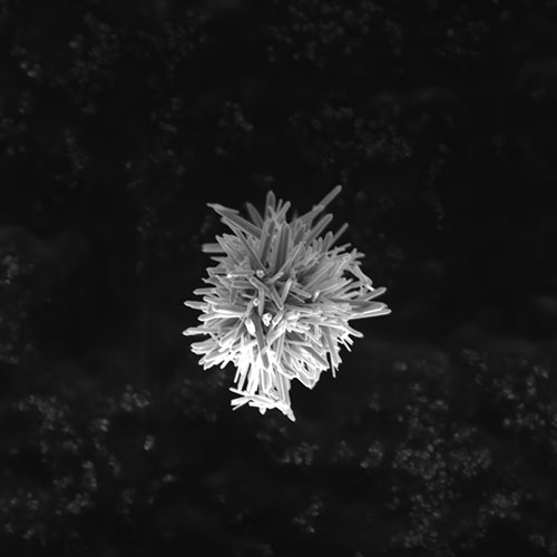
In this recent study published in Advanced Functional Materials, a team of scientists led by Martin Pumera have created a cost-effective way to destroy bacterial biofilms using light-driven, self-propelled micromotors (shown above). The micromotors were made with silver-doped zinc oxide, as both materials possess known antibacterial activity, and the self-propelling capabilities of the system enhances their diffusion to reach more bacteria. The researchers demonstrated their ability to eliminate both gram‐positive and gram‐negative bacteria biofilms from the solid surfaces, paving the way for advancements in everything from healthcare to utilities.
Injecting light
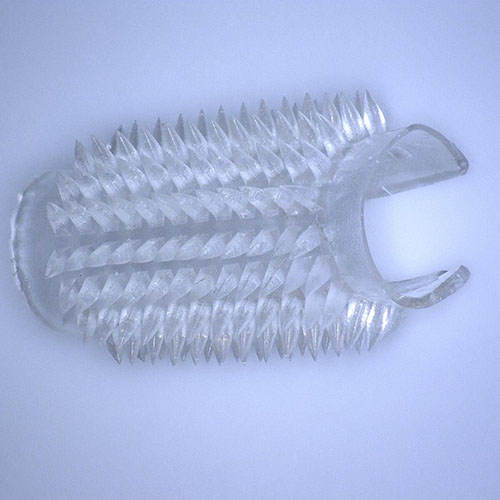
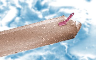
This strange looking spiky tube is actually a polymer microneedle array, not for the delivery of therapeutics into the skin, but for more targeted and guided deep penetration of light — like “injecting” light into the body. Phototherapy is a burgeoning field of research in healthcare and therapeutics, whilst microneedles are becoming increasingly important in the field of drug delivery. Combining these two fields of research, this microneedle array to help guide UV light deeper into the skin for treatment of dermatological conditions is the ingenious work of Shuai Xu, Bethany Perez White, John Rogers, and their co-workers, and is featured in Advanced Functional Materials. This wearable device could one day become a ubiquitous, inexpensive means of treating difficult skin conditions with phototherapy. Perhaps one day some of us may feel a little “flash” in the doctor’s office.
A better way to “interrogate” cells
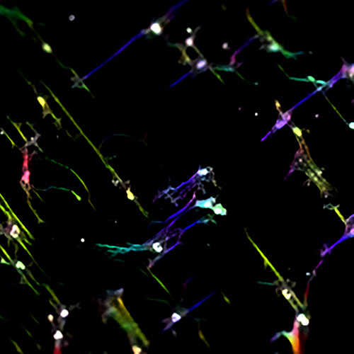
In native biological settings, cell development and behavior is driven by mechanical cues applied to the cells’ surface. Effectively reproducing this in a lab has been challenging because while causative effects between surface topography and cellular function have been demonstrated, the variability in materials used in this screening process makes them difficult to discern. In a paper published in Advanced Functional Materials, a team led by Victor Cadarso, Jessica Frith, and Nicolas Voelcker developed a new approach to imprinting micro‐ and nanoscale topographical features into the base of conventional cell culture-ware, facilitating the high‐throughput screening of 12 surface topographies and the resulting unique cell‐specific responses they elicit.
Next generation semi-conductors
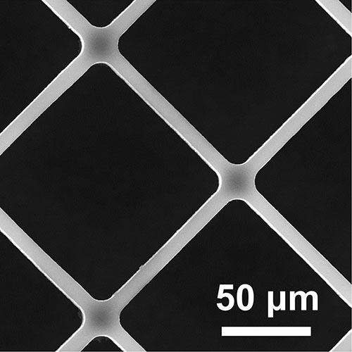
Single-crystalline silicon is one of the most common semiconductor materials in consumer electronics. One of the most common forms of this material is the “silicon wafer”, a material that is rigid, brittle and non-transparent. To address these drawbacks Jian-Sheng Jie, Xiao-Hong Zhang, and co-workers developed an elegant single-crystalline Si framework, imaged here using scanning electron microscopy, which is flexible, lightweight, tailorable, and highly transparent. Their findings were published this month in Advanced Materials.
See more in this series Science in pictures

