Reverse-biased silicon p–n junctions operating in avalanche breakdown mode emit light in the 400 to 900 nm range. This means that an optical coupling between such Si-LED and spectrally matched Si detectors integrated in an Si chip is possible, enabling transmission of information utilizing electrical/optical conversion of signals within the integrated optoelectronic system.
Previous work has demonstrated that Si-based light emitters (Si-diode LED) could operate in the GHz range and provide reliable operation, since the avalanche impact ionization process in semiconductors is generally considered to be an inherently very fast process.
However, in Si-diode LEDs, the speed of operation of avalanche breakdown is mainly determined by the discharge time that is equal to the product of on-resistance of the p–n junction in avalanche and the reverse-biased junction capacitance.
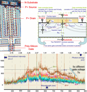
Alternatively, it is replaced with the discharge time of a metal-oxide-semiconductor (MOS) capacitor. Researchers from the State Key Laboratory of Electronic Thin Films and Integrated Devices in the University of Electronic Science and Technology of China, in this Phys. Status Solidi A article, have proposed a MOS-like device, utilizing the field effect of the gate in order to control the light emission from the reverse-biased p-n junction, by modifying its transition region electric field.
This can improve the Si-LED’s frequency response for both analog signal transmission and of switching speed for digital signal operations.
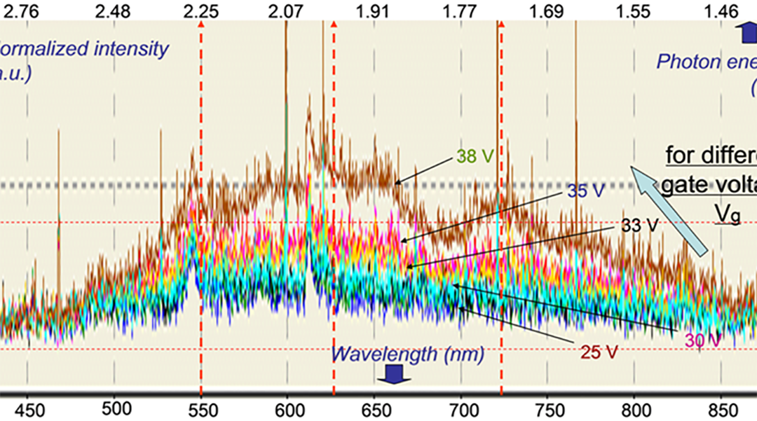
First, standard Si-CMOS process technology is utilized for fabricating the silicon optoelectronic device. The chip-based Si light emitting device with the MOS-structure emits a very broad electroluminescence spectrum with an expected wavelength range of 400 to 900 nm.
Since the gate-controlled capability is applied, the emitted light intensity is indeed dependent on the bias voltage of the insulated-gate terminal, resulting in the modulation of the light intensity by the gate voltage variation.
Second, the MOS-like structure essentially avoids the involvement of natural carrier lifetimes in the reverse-biased p-n junction with the discharge time of the p–n junction’s depletion layer capacitor-based LED.
The lifetime of the MOS-capacitor LED should be controllable via the capacitor discharge time. In other words, the Si gate-controlled diode LED operates on the principle of the MOS-capacitor and not on standard p–n junctions. In contrast to the lifetime of carriers in the depletion region, the MOS-capacitor discharge time also determines the modulation in the reverse-bias silicon p-n junction with gate control. Such a wonderful model referring to the MOS device structure, applied to all-silicon high-speed electro-optic modulation, is established as well.
Overall, the MOS-like diode utilizes the field effect induced by the gate for modulation of the diode’s space charge electric field and hence the optical output from the light emitting diode; the modulation speed for visible and infrared bands can attain higher frequencies with a significant offset.
The fabrication of the device is fully compatible with CMOS processing procedures. Therefore, the device can serve as an optical signal modulator in the high frequency range in the optoelectronic systems fabricated by the existing standard silicon technology. Such a high frequency in the GHz range represents a significant leap in silicon electro-optic modulator performance for future opto-electronic interconnects in the standard CMOS process.

Back cover for Phys. Status Solidi A., 2019, 216, 1970029
Kindly contributed by Kaikai Xu


