Image sensors for electronic devices are typically designed with bezels to provide structural integrity. Although bezels are becoming increasingly thinner, fabricating bezel-less, high-performance electronic devices with omnidirectional capability is a challenge.
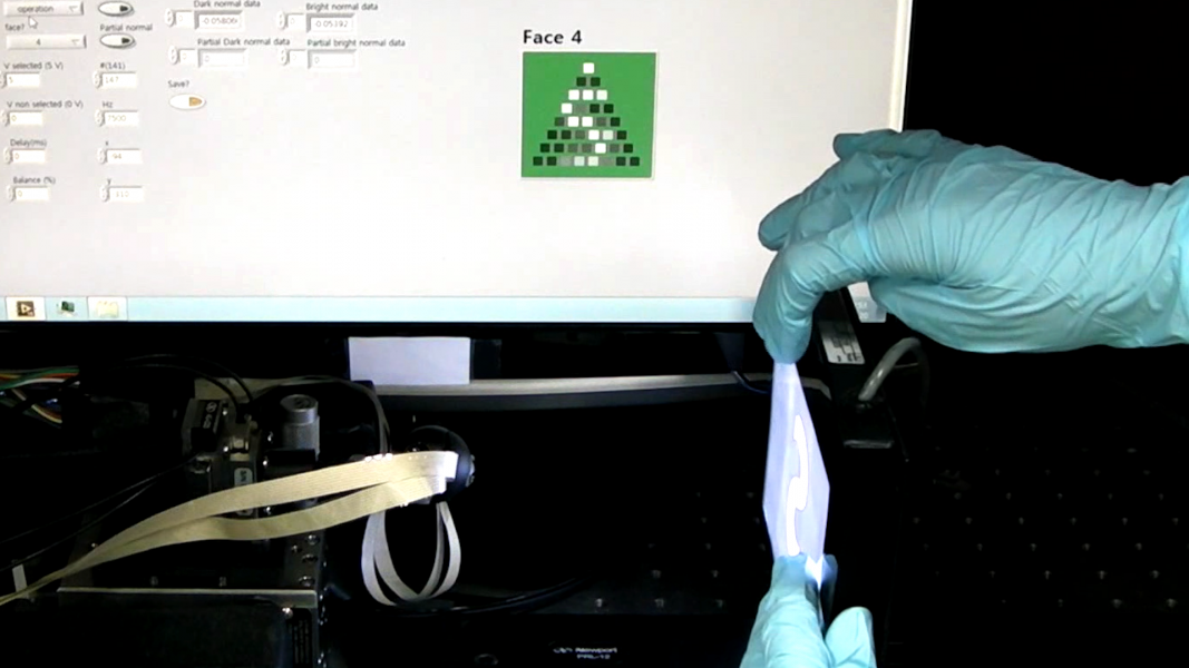
In their article in Advanced Materials, Prof. Heung Cho Ko and colleagues from Gwangju Institute of Science and Technology (GIST) present a strategy for placing bezel-less image sensors over the entire surface of a tetrahedral, 3D sensor.
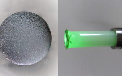
A multi-step process was used to produce triangular, printable silicon image sensors. These sensor components were laminated onto a 3D-printed acrylonitrile butadiene styrene framework and plasticized by exposure to acetone vapor. This surface-treated framework can be folded into a tetrahedron and mounted onto a spherical unit with four focal lenses.
Prof. Ko: “This method gives us a lot of freedom in aligning device layers. For example, when we align a planar device layer on the top surface of a plastic film, generally, extreme bending or folding causes too much stress, resulting in electrical failure. On the other hand, solvent-assisted plasticization prevents this behavior. Using this technology, we can develop three-dimensional sensors, displays, and other electronic devices from planar forms.”
Photoresponsive characteristics and performance of these bezel-less, tetrahedral image sensors yielded working pixels of 99.3% and demonstrated the omnidirectional capacity of these devices.
To find out more about this method for transforming planar electronic devices into 3D structures, please visit the Advanced Materials homepage.


