 From the discovery of graphene and its unique properties there has been enormous progress in the production of atomic crystals that are strictly two dimensional and can be viewed as individual planes of atomic-scale thickness pulled out of bulk crystals like graphite, h-BN, several transition metal dichalcogenides (TMDC), or complex oxides. By stacking various atomic crystals on top of each other it is possible to create multilayer heterostructures which hold the promise for novel devices with designed electronic properties. For instance, concepts for novel transistors based on lateral and vertical transport as well as optoelectronics have been demonstrated.
While obviously promising for applications, these new materials are very different from usual three dimensional bulk materials for several reasons. First, all atoms are now directly at a surface or some interface. Second, electrons are ultimately confined in atomically thin layers which make electronic properties extremely sensitive to structural details.
On a single particle level, vertical quantum confinement or stacking are known to control properties like electronic gaps. Importantly, atomic thickness and related confinement of electrons also lead to distinct many-body phenomena. Obviously, sensitivity to structural details means strong electron phonon coupling. In addition, Coulomb interaction is special in 2D materials due to reduced screening and quenching of kinetic energy in the vertical direction.
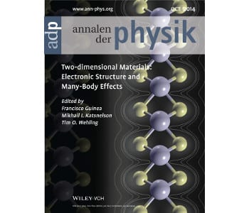
In other words, the electronic structure of 2D materials combines the issue of competing many-body interactions with sensitivity to atomistic structural details. This is why a coherent understanding of how to control the electronic and optical properties of new 2D materials and, particularly, a unifying “standard model” of their electronic structure remains yet to be built. A recent special issue of Annalen der Physik, guest-edited by Francisco Guinea, Mikhail I. Katsnelson, and Tim O. Wehling, is focused on the electronic structure, optical properties, interactions and collective phenomena in 2D materials.
Selected articles from the special issue:
Expert Opinion: Band structure and spin–orbit coupling engineering in transition-metal dichalcogenides by Jaroslav Fabian
Review Article: Electronic properties of single-layer and multilayer transition metal dichalcogenides MX2 (M = Mo, W and X = S, Se) by Rafael Roldán, Jose A. Silva-Guillén, M. Pilar López-Sancho, Francisco Guinea, Emmanuele Cappelluti and Pablo Ordejón


