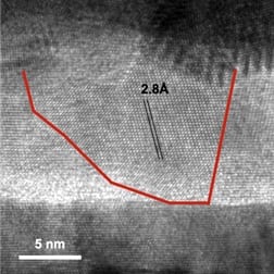
Most metal oxide materials commonly demonstrate resistance change when electrical voltage is applied. It was first reported in early 1960’s and has long been a mysterious problem; however, it was forgotten for a long time due to the difficulties in revealing more details. Early 2000’s, it was revisited due to the potential in memory applications. In addition, it was proposed as a memristor, which could be used as an electrical circuit element in various ways. Attributed to the advancement of modern characterization tools and extensive investigations, the filamentary model, generation and rupture of conducting paths across the sandwiched metal oxide between metal electrodes, has been experimentally proven.
 The nature of a filament is a key to understand resistive switching phenomena. However, the physical structure of the filament is still unclear because of limited direct evidences. Even for a model oxide system of NiO which has been studied extensively, experimental evidences of its filament structure are incomplete or contradictory.
In their recent work in physica status solidi RRL Professor Miyoung Kim and Dr. Deok-Hwang Kwon propose a Ni2O3 phase as a highly possible filament structure. The Ni2O3 phase was directly observed by high-resolution transmission electron microscopy in the unipolar NiO thin films by comparing low resistance state and high resistance state samples. This observation complies with the fact that a Ni vacancy is an active defect rather than an oxygen vacancy in the NiO material, known as a p-type semiconductor. This report indicates that the formation and rupture of a filament would be related to active defects in each different oxide systems, not simply oxygen vacancies.
The text is kindly provided by Miyoung Kim.


