 Welcome to one of our guest columns, where active researchers can share their views on topics relevant to materials science. Professor Geoffrey Ozin from the University of Toronto shares his thoughts on the sensor applications of nanomaterials.
It seems these days that if one’s “pet nanomaterial” does not live up to initial expectations for use as an active component of a solar cell, photodetector, light-emitting diode, laser, field-effect transistor, battery, display, chromatography stationary phase, water splitting or carbon dioxide recycling photocatalyst, hydrogen storage or gas separation open framework, drug delivery or detoxification system, medical imaging or therapeutic device, then for sure it will respond in some way to some stimulus and thereby function as some sort of chemical or biological sensor.
Is this the nano-graveyard for our beloved nanomaterials? A kind of nanoscience ‘booby’ prize often claimed by researchers who discover that their materials are unsuitable for their initially intended uses? Or is it rather a valid scientific and novel application, and is nanochemistry the place to look for the sensors of the future, or will it only provide us with a stream of barely adequate also-rans?
The glass pH electrode invented by W. S. Hughes in 1922 is the first recorded chemical sensor. Here the pH of a solution is detected through chemical exchange signals in a thin glass membrane. This breakthrough was followed by a stream of other kinds of sensors for detecting a variety of chemicals from oxygen to glucose. Developments in the semiconductor microelectronics industry led to the miniaturization of circuits and sensor arrays in the 1980s that were able to exploit signal pattern recognition for differentiating different chemicals and biochemicals.
Around this time nanochemistry was beginning to produce myriad examples of nanocrystals and nanowires with controlled size and shape with surfaces that could be chemically modified to make them function as new sensor platforms for monitoring chemical and biochemical contaminants in water, air and food, as well as biomedical and security applications.
The large surface-to-volume ratio of these nanomaterials meant that minute changes in their environment could trigger a detectable response to just a single molecule; exemplified by surface enhanced Raman spectroscopy, Förster resonance energy transfer and whispering gallery optical microcavity techniques. Additionally, these materials’ small size meant that they could provide a unique opportunity to sense the environment in nanoscale spaces like that found in a living cell or even a cell nucleus. Through intelligent design of chemical and biochemical molecular recognition events between receptor and analyte at the surface of a nanocrystal or nanowire, coupled with large optical and electrical responses to these events, it has been proven possible to develop a wealth of new highly selective and sensitive sensors able to monitor heavy metals in drinking water, detect bacteria and viruses in our hospitals, indicate when food has spoiled and identify chemical and biological agents in acts of war and terrorism.
But the search for nanochemistry-inspired sensors is often the pursuit of last resort that researchers adopt with their nanomaterials platform when they have run out of ideas. This is because pretty well any nanomaterial will show a response to a stimulus and therefore function as a sensor – is it the death of imagination?
A genuinely novel nanomaterial sensing mechanism is worthy of exploration but too much effort goes into trying to improve sensor performance by a few tenths of a percent rather than to searching for real breakthroughs. Unfortunately this same situation is present in many other areas of science, such as much of today’s energy nanomaterials research.
So what is next for nanochemical and biochemical sensor research? Should we not be trying as hard as possible to find something absolutely outrageous to do? Something crazy that might just work? Shouldn’t we be trying to find the next glass pH electrode, rather than trying to squeeze that extra fraction of a percent out of our tried and tested materials?
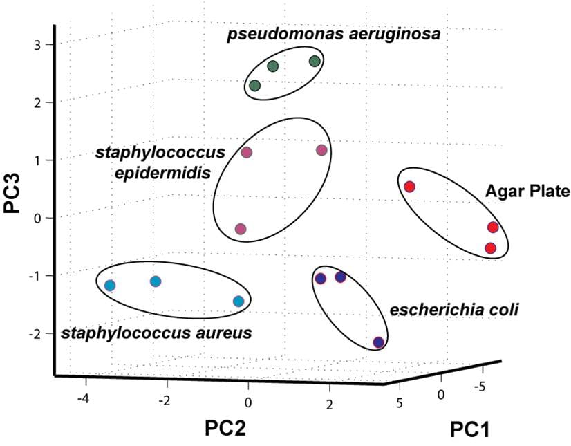
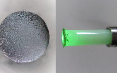
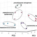
An example of a new type of sensor, which is close to my heart and which certainly falls into the crazy category and is showing great promise for actual commercial application, is a pixelated nanoparticle one-dimensional photonic crystal chip in which each pixel is functionalized with different molecule recognition sites that display diagnostic color changes when exposed to different vapor phase analytes; a ‘photonic nose’, if you will [1]. The overall photonic color response of the chip to the headspace atmosphere of bacteria, recorded with a simple digital camera color image with automated principal component (color image change) analysis, enabled distinct strains of bacteria to be distinguished (see above image). This breakthrough was achieved by Leonardo Bonifacio, a recently graduated coworker in my research group, who is actively involved in commercializing the P-Nose platform at the University of Toronto. The next stage of development will allow for a portable, versatile and low-cost sensing platform with potential for applications that span from environmental monitoring to food safety to disease diagnostics.
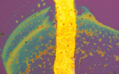
Another amazing and ‘crazy’ (and I mean that in the best possible way) – sensor, from the laboratory of Shana Kelly, also at the University of Toronto [2]. She is also commercially developing an array of on-chip nanostructured palladium sensing nanoelectrodes. The location of these nanoelectrodes is defined by top-down nanolithography, their growth is enabled by bottom-up nanochemistry and their surfaces are functionalized with biomolecule recognition agents using thiol chemical anchoring strategies. Attomolar sensitivity in a proof-of-concept nucleic acid assay has been realized with finely-structured highly-branched nanoelectrodes that provide to analytes high surface area coral-, cauliflower- and snowflake-like nanoscale “natural” forms. The impressive sensitivity of these tiny electrochemical sensors seems to be related to their nanostructuring and their capacity for genetic analysis of cancer cells, as well as detection of proteins, RNA and DNA, bodes well for their implementation in high-throughput, high-performance medical diagnostics.
How about getting nanomaterials smarter and a bit crazier? That is what Mike Sailor at UC San Diego has been doing by developing a ‘smart dust’ [3]. Also based on photonic crystals, these platforms are strong competitors for remote detection of threat agents and toxic chemicals. The grains of ‘dust’ are actually tiny particles composed of nanoporous photonic crystals usually made of silicon that change color in the presence of certain compounds. The material can be sprayed onto a surface and the color change can be monitored remotely by use of a portable laser source with an integrated detection system. In this way, a hazard can be detected at a remote location even before anybody has entered the space.
These are just a few examples of technologies based on nanochemistry that are going beyond academic curiosities. They are actually getting closer and closer to real world applications. Some nanomaterials are really learning how to navigate the rough path towards the sensing market!
Now that’s really crazy and pretty impressive too!!!
Image credit: L. D. Bonifacio, PhD Dissertation, University of Toronto
[1] L. D. Bonifacio, D. P. Puzzo, B. M Willey, U. Kamp, A. McGeer, G. A. O
zin, “Towards the Photonic Nose: A Novel Platform for Molecule to Bacteria Identification,” Advanced Materials 2010, 22, 1351-1354
[2] L. Soleymani, Z. Fang, E. H. Sargent, S. O. Kelley, “Programming the Detection Limits of Biosensors through Controlled Nanostructuring,” Nature Nanotechnology 2009, 4, 844-848.
[3] M. J. Sailor, “Color Me Sensitive: Amplification and Discrimination in Photonic Silicon Nanostructures,” ACS Nano 2007, 1, 248-252.

